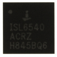
ISL8118IRZ Intersil, ISL8118IRZ Datasheet - Page 15

ISL8118IRZ
Manufacturer Part Number
ISL8118IRZ
Description
IC CTRLR PWM 1-PHASE 28-QFN
Manufacturer
Intersil
Datasheet
1.ISL8118CRZ.pdf
(20 pages)
Specifications of ISL8118IRZ
Pwm Type
Voltage Mode
Number Of Outputs
1
Frequency - Max
2MHz
Duty Cycle
100%
Voltage - Supply
2.97 V ~ 22 V
Buck
Yes
Boost
No
Flyback
No
Inverting
No
Doubler
No
Divider
No
Cuk
No
Isolated
No
Operating Temperature
-40°C ~ 85°C
Package / Case
28-VQFN Exposed Pad, 28-HVQFN, 28-SQFN, 28-DHVQFN
Frequency-max
2MHz
Rohs Compliant
YES
Lead Free Status / RoHS Status
Lead free / RoHS Compliant
Available stocks
Company
Part Number
Manufacturer
Quantity
Price
Company:
Part Number:
ISL8118IRZ
Manufacturer:
Intersil
Quantity:
120
Part Number:
ISL8118IRZ
Manufacturer:
INTERSIL
Quantity:
20 000
As the VDIFF pin is connected internally to the
OV/UV/PGOOD comparator, an external resistor divider
must then be connected to VDIFF to provide correct voltage
information for the OV/UV comparator. An RC filter should
be used if VDIFF is to be connected directly to FB instead of
to VOUT through a separate resistor divider network. This
filter prevents noise injection from disturbing the
OV/UV/PGOOD comparators on VDIFF. VDIFF may also be
connected to the SS pin, which completely bypasses the
OV/UV/PGOOD functionality.
Application Guidelines
Layout Considerations
As in any high frequency switching converter, layout is very
important. Switching current from one power device to
another can generate voltage transients across the
impedances of the interconnecting bond wires and circuit
traces. These interconnecting impedances should be
minimized by using wide, short printed circuit traces. The
critical components should be located as close together as
possible using ground plane construction or single point
grounding.
Figure 7 shows the critical power components of the
converter. To minimize the voltage overshoot/undershoot the
interconnecting wires indicated by heavy lines should be part
of ground or power plane in a printed circuit board. The
components shown in Figure 8 should be located as close
together as possible. Please note that the capacitors CIN
and CO each represent numerous physical capacitors.
Locate the ISL8118 within 3 inches of the MOSFETs, Q1 and
Q2. The circuit traces for the MOSFETs’ gate and source
connections from the ISL8118 must be sized to handle up to
4A peak current.
VOUT (LOCAL)
GND (LOCAL)
FIGURE 6. SIMPLIFIED UNITY GAIN DIFFERENITAL SENSING IMPLEMENTATION
15
800mV
VCC
10Ω
10Ω
(REMOTE)
VSENSE-
VSENSN
R
C
OS
SEN
(REMOTE)
VSENSE+
VSENSP
ISL8118
R
GAIN = 1
FB
V
SS
Proper grounding of the IC is important for correct operation in
noisy environments. The PGND pin should be connected to
board ground at the source of the bottom side MOSFET with a
wide short trace. The GND pin should be connected to a large
copper fill under the IC which is subsequently connected to
board ground at a quite location on the board, typically found
at an input or output bulk (electrolytic) capacitor.
VDIFF
ISL8118
FIGURE 7. PRINTED CIRCUIT BOARD POWER AND
FIGURE 8. PRINTED CIRCUIT BOARD SMALL SIGNAL
C
SS
SS
Z
OV/UV
COMP
IN
GND
BGATE
TGATE
ISL8118
PGND
GROUND PLANES OR ISLANDS
LAYOUT GUIDELINES
LX
ERROR AMP
FB
PGND
Z
FB
LX
C
PVCC
BOOT
BOOT
+5V
V
Q2
Q1
RETURN
COMP
IN
C
PVCC
D1
C
Q1
+V
Q2
IN
IN
L
L
O
O
C
C
O
O
V
OUT
April 7, 2009
V
FN6325.1
OUT


