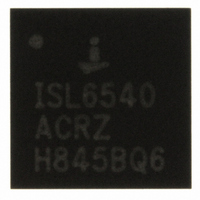
ISL8118IRZ Intersil, ISL8118IRZ Datasheet - Page 13

ISL8118IRZ
Manufacturer Part Number
ISL8118IRZ
Description
IC CTRLR PWM 1-PHASE 28-QFN
Manufacturer
Intersil
Datasheet
1.ISL8118CRZ.pdf
(20 pages)
Specifications of ISL8118IRZ
Pwm Type
Voltage Mode
Number Of Outputs
1
Frequency - Max
2MHz
Duty Cycle
100%
Voltage - Supply
2.97 V ~ 22 V
Buck
Yes
Boost
No
Flyback
No
Inverting
No
Doubler
No
Divider
No
Cuk
No
Isolated
No
Operating Temperature
-40°C ~ 85°C
Package / Case
28-VQFN Exposed Pad, 28-HVQFN, 28-SQFN, 28-DHVQFN
Frequency-max
2MHz
Rohs Compliant
YES
Lead Free Status / RoHS Status
Lead free / RoHS Compliant
Available stocks
Company
Part Number
Manufacturer
Quantity
Price
Company:
Part Number:
ISL8118IRZ
Manufacturer:
Intersil
Quantity:
120
Part Number:
ISL8118IRZ
Manufacturer:
INTERSIL
Quantity:
20 000
Sinking OCP faults cause the bottom side MOSFET drive to
be disabled, effectively operating the ISL8118 in a
non-synchronous manner. The fault is maintained for three
clock cycles at which point it is cleared and normal operation
is restored. OVP fault implementation overrides sourcing
and sinking OCP events, immediately turning on the bottom
side MOSFET and turning off the top side MOSFET. The OC
trip point varies mainly due to the MOSFETs rDS(ON)
variations and system noise. To avoid overcurrent tripping in
the normal operating load range, find the RTSOC and/or
RBSOC resistor from the previous detailed equations with:
Frequency Programming
By tying a resistor to GND from FSET pin, the switching
frequency can be set between 250kHz and 2MHz.
Oscillator/VFF
The Oscillator is a triangle waveform, providing for leading
and falling edge modulation. The bottom of the oscillator
waveform is set at 1.0V. The ramp's peak-to-peak amplitude
is determined from the voltage on the VFF (Voltage Feed
Forward) pin by Equation 1:
An internal RC filter of 233kΩ and 2pF (341kHz) provides
filtering of the VFF voltage. An external RC filter may be
required to augment this filter in the event that it is insufficient to
prevent noise injection or control loop interactions. Voltages
below 2.9V on the VFF pin may result in undesirable operation
due to extremely small peak-to-peak oscillator waveforms. The
oscillator waveform should not exceed VCC -1.0V. For high
VFF voltages the internal/external 5.6V linear regulator should
be used. 5.6V on VCC provides sufficient headroom for 100%
duty cycle operation when using the maximum VFF voltage of
22V. In the event of sustained 100% duty cycle operation,
defined as 32 clock cycles where no BG pulse is detected, BG
will be pulsed on to refresh the design’s Bootstrap capacitor.
D
1. Maximum rDS(ON) at the highest junction temperature;
2. Minimum IBSOC and/or ITSOC from specification table;
3. Determine the overcurrent trip point greater than the
VOSC
maximum output continuous current at maximum
inductor ripple current.
100
10
FIGURE 4. R
=
1
100k
0.16 VFF
•
FS
RESISTANCE vs FREQUENCY
FREQUENCY (Hz)
13
1M
(EQ. 1)
10M
ISL8118
Internal Series Linear Regulator
The VIN pin is connected to PVCC with a 2Ω internal series
linear regulator, which is internally compensated. The external
Series Linear regulator option should be used for applications
requiring pass elements of less than 2Ω. When using the
internal regulator, the EXDRV pin should be connected directly
to GND. The PVCC and VIN pins should have a bypass
capacitor (at least 10µF on PVCC is required) connected to
PGND. For proper operation, the PVCC capacitor must be
within 150 mils of the PVCC and the PGND pins, and be
connected to these pins with dedicated traces. The internal
series linear regulator’s input (VIN) can range between 3.3V to
20V ±10%. The internal linear regulator is to provide power for
both the internal MOSFET drivers through the PVCC pin and
the analog circuitry through the VCC pin. The VCC pin should
be connected to the PVCC pin with an RC filter to prevent high
frequency driver switching noise from entering the analog
circuitry. When VIN drops below 5.6V, the pass element will
saturate; PVCC will track VIN, minus the dropout of the linear
regulator: PVCC = VIN-2xIVIN. When used with an external 5V
supply, the VIN pin should be tied directly to PVCC.
External Series Linear Regulator
The EXDRV pin provides sinking drive capability for an
external pass element linear regulator controller. The
external linear options are especially useful when the
internal linear dropout is too large for a given application.
When using the external linear regulator option, the EXDRV
pin should be connected to the gate of a PMOS device, and
a resistor should be connected between its gate and source.
A resistor and a capacitor should be connected from gate to
source to compensate the control loop. A PNP device can be
used instead of a PMOS device, in which case the EXDRV
pin should be connected to the base of the PNP pass
element. The maximum sinking capability of the EXDRV pin
is 0.5mA, and should not be exceeded if using an external
resistor for a PMOS device. The designer should take care
in designing a stable system when using external pass
elements. The VCC pin should be connected to the PVCC
pin with an RC filter to prevent high frequency driver
switching noise from entering the analog circuitry.
High Speed MOSFET Gate Driver
The integrated driver has similar drive capability and features
to Intersil's ISL6605 stand alone gate driver. The PWM
tri-state feature helps prevent a negative transient on the
output voltage when the output is being shut down. This
eliminates the Schottky diode that is used in some systems for
protecting the microprocessor from reversed-output-voltage
damage. See the ISL6605 datasheet for specification
parameters that are not defined in the current ISL8118
Electrical Specifications table.
Fs Hz
[
]
≈
1.178
×10
10
•
R
T
[ ]
Ω
–
0.973
(R
T
TO GND)
April 7, 2009
(EQ. 2)
FN6325.1


