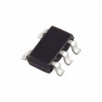
ADR395BUJZ-R2 Analog Devices Inc, ADR395BUJZ-R2 Datasheet - Page 17

ADR395BUJZ-R2
Manufacturer Part Number
ADR395BUJZ-R2
Description
IC VREF W/SHUTDN 5V TSOT23-5
Manufacturer
Analog Devices Inc
Series
ADR39r
Datasheet
1.ADR395AUJZ-REEL7.pdf
(20 pages)
Specifications of ADR395BUJZ-R2
Temperature Coefficient
9ppm/°C
Reference Type
Series
Voltage - Output
5V
Tolerance
±0.1%
Voltage - Input
5.3 ~ 15 V
Number Of Channels
1
Current - Quiescent
140µA
Current - Output
5mA
Operating Temperature
-40°C ~ 125°C
Mounting Type
Surface Mount
Package / Case
TSOT-23-5, TSOT-5, TSOP-5
Topology
Series
Input Voltage
4.3V To 15V
Reference Voltage
5V
Reference Voltage Tolerance
5mV
Voltage Reference Case Style
TSOT
No. Of Pins
5
Lead Free Status / RoHS Status
Lead free / RoHS Compliant
Current - Cathode
-
Lead Free Status / RoHS Status
Lead free / RoHS Compliant, Lead free / RoHS Compliant
APPLICATIONS INFORMATION
BASIC VOLTAGE REFERENCE CONNECTION
The circuit shown in Figure 40 illustrates the basic configuration
for the ADR39x family. Decoupling capacitors are not required
for circuit stability. The ADR39x family is capable of driving
capacitive loads from 0 μF to 10 μF. However, a 0.1 μF ceramic
output capacitor is recommended to absorb and deliver the
charge, as required by a dynamic load.
Stacking Reference ICs for Arbitrary Outputs
Some applications may require two reference voltage sources,
which are a combined sum of standard outputs. Figure 41 shows
how this stacked output reference can be implemented.
Two reference ICs are used, fed from an unregulated input,
V
which provide two output voltages, V
terminal voltage of U1, while V
and the terminal voltage of U2. U1 and U2 are chosen for the
two voltages that supply the required outputs (see the Output
IN
. The outputs of the individual ICs are connected in series,
SHUTDOWN
*NOT REQUIRED
V
IN
INPUT
Figure 40. Basic Configuration for the ADR39x Family
Figure 41. Stacking Voltage References with the
C
B
0.1µF
0.1 µF
ADR390/ADR390
ADR391/ADR391
ADR392/ADR392
ADR395/ADR395
*
ADR390/ADR391/ADR392/ADR395
0.1µF
C2
C2
U1/U2
OUTPUT TABLE
SHDN
SHDN
SHDN
V
V
V
V
V
V
IN
OUT (SENSE)
V
2.048
2.5
4.096
5
OUT (FORCE)
OUT (SENSE)
OUT (FORCE)
OUT (SENSE)
OUT1
ADR39x
OUT2
V
GND
GND
OUT (FORCE)
V
V
IN
IN
(V) V
is the sum of this voltage
U2
U1
OUT1
GND
4.096
5.0
8.192
10
OUT2
and V
C
(V)
B
*
0.1µF
OUT2
OUTPUT
V
. V
V
OUT2
OUT1
OUT1
is the
Rev. G | Page 17 of 20
Table in Figure 41). For example, if both U1 and U2 are
ADR391s, V
While this concept is simple, a precaution is required. Because
the lower reference circuit must sink a small bias current from
U2 plus the base current from the series PNP output transistor
in U2, either the external load of U1 or an external resistor must
provide a path for this current. If the U1 minimum load is not
well defined, the external resistor should be used and set to a
value that conservatively passes 600 μA of current with the
applicable V
reference circuits are treated locally as macrocells; each has its
own bypasses at input and output for best stability. Both U1 and
U2 in this circuit can source dc currents up to their full rating.
The minimum input voltage, V
the outputs, V
A Negative Precision Reference without Precision Resistors
A negative reference can be easily generated by adding an A1
op amp and is configured as shown in Figure 42. V
and V
reference can be taken directly from the output of the op amp.
The op amp must be dual-supply, low offset, and rail-to-rail if
the negative supply voltage is close to the reference output.
General-Purpose Current Source
Many times in low power applications, the need arises for
a precision current source that can operate on low supply
voltages. The ADR390/ADR391/ADR392/ADR395 can be
configured as a precision current source. As shown in Figure 43,
the circuit configuration is a floating current source with a
grounded load. The reference output voltage is bootstrapped
across R
this configuration, circuit precision is maintained for load
currents in the range from the reference supply current,
typically 90 μA to approximately 5 mA.
OUT (SENSE)
SET
ADR390/ADR391/ADR392/ADR395
, which sets the output current into the load. With
OUT1
OUT1
OUT2
are at virtual ground and, therefore, the negative
across it. Note that the two U1 and U2
is 2.5 V and V
–V
A1
, plus the dropout voltage of U2.
DD
Figure 42. Negative Reference
V
V
OUT (FORCE)
OUT (SENSE)
+V
OUT2
IN
GND
V
, is determined by the sum of
IN
DD
SHDN
is 5.0 V.
–V
REF
OUT (FORCE)


