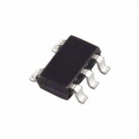
ADR395BUJZ-R2 Analog Devices Inc, ADR395BUJZ-R2 Datasheet - Page 16

ADR395BUJZ-R2
Manufacturer Part Number
ADR395BUJZ-R2
Description
IC VREF W/SHUTDN 5V TSOT23-5
Manufacturer
Analog Devices Inc
Series
ADR39r
Datasheet
1.ADR395AUJZ-REEL7.pdf
(20 pages)
Specifications of ADR395BUJZ-R2
Temperature Coefficient
9ppm/°C
Reference Type
Series
Voltage - Output
5V
Tolerance
±0.1%
Voltage - Input
5.3 ~ 15 V
Number Of Channels
1
Current - Quiescent
140µA
Current - Output
5mA
Operating Temperature
-40°C ~ 125°C
Mounting Type
Surface Mount
Package / Case
TSOT-23-5, TSOT-5, TSOP-5
Topology
Series
Input Voltage
4.3V To 15V
Reference Voltage
5V
Reference Voltage Tolerance
5mV
Voltage Reference Case Style
TSOT
No. Of Pins
5
Lead Free Status / RoHS Status
Lead free / RoHS Compliant
Current - Cathode
-
Lead Free Status / RoHS Status
Lead free / RoHS Compliant, Lead free / RoHS Compliant
ADR390/ADR391/ADR392/ADR395
THEORY OF OPERATION
Band gap references are the high performance solution for low
supply voltage and low power voltage reference applications,
and the ADR390/ADR391/ADR392/ADR395 are no exception.
The uniqueness of these devices lies in the architecture. As
shown in Figure 39, the ideal zero TC band gap voltage is
referenced to the output, not to ground. Therefore, if noise
exists on the ground line, it is greatly attenuated on V
band gap cell consists of the PNP pair, Q51 and Q52, running at
unequal current densities. The difference in V
voltage with a positive TC, which is amplified by a ratio of
This PTAT voltage, combined with V
produces a stable band gap voltage.
Reduction in the band gap curvature is performed by the ratio
of Resistors R44 and R59, one of which is linearly temperature
dependent. Precision laser trimming and other patented circuit
techniques are used to further enhance the drift performance.
2 ×
SHDN
R58
R54
Figure 39. Simplified Schematic
R59
R54
R60
Q51
Q1
R53
R58
Q52
R44
R61
R48
R49
BE
s of Q51 and Q52,
V
V
V
GND
OUT (FORCE)
OUT (SENSE)
IN
BE
results in a
OUT
. The
Rev. G | Page 16 of 20
DEVICE POWER DISSIPATION CONSIDERATIONS
The ADR390/ADR391/ADR392/ADR395 are capable of
delivering load currents to 5 mA, with an input voltage that
ranges from 2.8 V (ADR391 only) to 15 V. When these devices
are used in applications with large input voltages, care should be
taken to avoid exceeding the specified maximum power
dissipation or junction temperature because it could result in
premature device failure. The following formula should be used
to calculate the maximum junction temperature or dissipation
of the device:
where:
T
P
θ
SHUTDOWN MODE OPERATION
The ADR390/ADR391/ADR392/ADR395 include a shutdown
feature that is TTL/CMOS level compatible. A logic low or a
zero volt condition on the SHDN pin is required to turn the
devices off. During shutdown, the output of the reference
becomes a high impedance state, where its potential would then
be determined by external circuitry. If the shutdown feature is
not used, the SHDN pin should be connected to V
JA
D
J
and T
is the device power dissipation.
is the device package thermal resistance.
P
D
A
=
are, respectively, the junction and ambient temperatures.
T
J
θ
–
JA
T
A
IN
(Pin 2).
(5)


