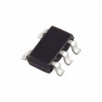
ADR395BUJZ-R2 Analog Devices Inc, ADR395BUJZ-R2 Datasheet

ADR395BUJZ-R2
Specifications of ADR395BUJZ-R2
Related parts for ADR395BUJZ-R2
ADR395BUJZ-R2 Summary of contents
Page 1
FEATURES Compact 5-lead TSOT packages Low temperature coefficient B grade: 9 ppm/°C A grade: 25 ppm/°C Initial accuracy B grade: ±4 mV maximum (ADR390) A grade: ±6 mV maximum Ultralow output noise: 5 μV p-p (0 Hz) ...
Page 2
ADR390/ADR391/ADR392/ADR395 TABLE OF CONTENTS Features .............................................................................................. 1 Applications ....................................................................................... 1 Pin Configuration ............................................................................. 1 General Description ......................................................................... 1 Specifications ..................................................................................... 3 ADR390 Electrical Characteristics ............................................. 3 ADR391 Electrical Characteristics ............................................. 4 ADR392 Electrical Characteristics ............................................. 5 ADR395 Electrical Characteristics ............................................. ...
Page 3
SPECIFICATIONS ADR390 ELECTRICAL CHARACTERISTICS 25°C, unless otherwise noted Table 2. Parameter Symbol OUTPUT VOLTAGE INITIAL ACCURACY V OERR V OERR V OERR V OERR TEMPERATURE ...
Page 4
ADR390/ADR391/ADR392/ADR395 ADR391 ELECTRICAL CHARACTERISTICS 25°C, unless otherwise noted Table 3. Parameter Symbol OUTPUT VOLTAGE INITIAL ACCURACY V OERR V OERR V OERR V OERR TEMPERATURE ...
Page 5
ADR392 ELECTRICAL CHARACTERISTICS 25°C, unless otherwise noted Table 4. Parameter Symbol OUTPUT VOLTAGE INITIAL ACCURACY V OERR V OERR V OERR V OERR TEMPERATURE COEFFICIENT ...
Page 6
ADR390/ADR391/ADR392/ADR395 ADR395 ELECTRICAL CHARACTERISTICS 25°C, unless otherwise noted Table 5. Parameter Symbol OUTPUT VOLTAGE INITIAL ACCURACY V OERR V OERR V OERR V OERR TEMPERATURE ...
Page 7
ABSOLUTE MAXIMUM RATINGS At 25°C, unless otherwise noted. Table 6. Parameter Supply Voltage Output Short-Circuit Duration to GND Storage Temperature Range Operating Temperature Range Junction Temperature Range Lead Temperature (Soldering, 60 sec) Stresses above those listed under Absolute Maximum Ratings ...
Page 8
ADR390/ADR391/ADR392/ADR395 TERMINOLOGY Temperature Coefficient The change of output voltage with respect to operating temper- ature changes normalized by the output voltage at 25°C. This parameter is expressed in ppm/°C and can be determined by the following equation ...
Page 9
TYPICAL PERFORMANCE CHARACTERISTICS 2.060 2.056 SAMPLE 2 2.052 2.048 SAMPLE 1 2.044 2.040 –40 –5 30 TEMPERATURE (°C) Figure 2. ADR390 Output Voltage vs. Temperature 2.506 2.504 SAMPLE 1 2.502 2.500 2.498 2.496 2.494 –40 –5 30 TEMPERATURE (°C) Figure ...
Page 10
ADR390/ADR391/ADR392/ADR395 140 +125°C 120 100 +25°C –40° INPUT VOLTAGE (V) Figure 8. ADR392 Supply Current vs. Input Voltage 140 +125 ° C 120 +25 ° C 100 –40 ° ...
Page 11
TEMPERATURE (°C) Figure 14. ADR390 Line Regulation vs. Temperature –40 – TEMPERATURE (°C) Figure 15. ADR391 Line Regulation vs. Temperature ...
Page 12
ADR390/ADR391/ADR392/ADR395 4.8 4.6 4.4 4.2 4.0 3 LOAD CURRENT (mA) Figure 20. ADR392 Minimum Input Voltage vs. Load Current 6.0 5.8 5.6 5.4 5.2 5.0 4.8 4 LOAD CURRENT (mA) Figure 21. ...
Page 13
TIME (10µs/DIV) Figure 26. ADR391 Voltage Noise kHz C BYPASS LINE 0.5V/DIV INTERRUPTION V 1V/DIV OUT TIME (10µs/DIV) Figure 27. ADR391 Line Transient Response C BYPASS 0.5V/DIV LINE INTERRUPTION V OUT 1V/DIV Figure 28. ADR391 Line ...
Page 14
ADR390/ADR391/ADR392/ADR395 V = 15V IN 5V/DIV V IN 2V/DIV V OUT TIME (20µs/DIV) Figure 32. ADR391 Turn-On Response Time 15V IN V 5V/DIV IN V 2V/DIV OUT TIME (40µs/DIV) Figure 33. ADR391 Turn-Off Response at ...
Page 15
R = 500Ω 100nF L 2V/DIV V OUT 5V/DIV V IN TIME (200 µs/DIV) Figure 36. ADR391 Turn-On/Turn-Off Response –20 –40 –60 –80 –100 –120 10 100 1k 10k ...
Page 16
ADR390/ADR391/ADR392/ADR395 THEORY OF OPERATION Band gap references are the high performance solution for low supply voltage and low power voltage reference applications, and the ADR390/ADR391/ADR392/ADR395 are no exception. The uniqueness of these devices lies in the architecture. As shown in ...
Page 17
APPLICATIONS INFORMATION BASIC VOLTAGE REFERENCE CONNECTION The circuit shown in Figure 40 illustrates the basic configuration for the ADR39x family. Decoupling capacitors are not required for circuit stability. The ADR39x family is capable of driving capacitive loads from 0 μF ...
Page 18
ADR390/ADR391/ADR392/ADR395 V IN SHDN V OUT (SENSE) ADR39x OUT (FORCE) 0.1µF R1 GND I SY ADJUST SET R Figure 43. A General-Purpose Current Source High Power Performance with Current Limit In some cases, ...
Page 19
... ADR392BUJZ-REEL7 4.096 ±5 1 ADR392BUJZ-R2 4.096 ±5 1 ADR395AUJZ-REEL7 5.0 ±6 1 ADR395AUJZ-R2 5.0 ±6 1 ADR395BUJZ-REEL7 5.0 ±5 1 ADR395BUJZ-R2 5.0 ± RoHS Compliant Part. 2.90 BSC 5 4 2.80 BSC 1.60 BSC PIN 1 0.95 BSC 1.90 BSC * 1.00 MAX 0.20 0.08 0.50 SEATING PLANE ...
Page 20
ADR390/ADR391/ADR392/ADR395 NOTES ©2002–2008 Analog Devices, Inc. All rights reserved. Trademarks and registered trademarks are the property of their respective owners. D00419-0-2/08(G) Rev Page ...


