AD652JP Analog Devices Inc, AD652JP Datasheet - Page 12
AD652JP
Manufacturer Part Number
AD652JP
Description
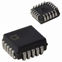
IC V-F CONV SYNCH MONO 5V 20PLCC
Manufacturer
Analog Devices Inc
Type
Voltage to Frequencyr
Datasheet
1.AD652JPZ.pdf
(28 pages)
Specifications of AD652JP
Rohs Status
RoHS non-compliant
Frequency - Max
2MHz
Full Scale
±25ppm/°C
Linearity
±0.005%
Mounting Type
Surface Mount
Package / Case
20-LCC (J-Lead)
Converter Function
VFC
Full Scale Frequency
2000
Power Supply Requirement
Single/Dual
Single Supply Voltage (max)
36V
Single Supply Voltage (min)
12V
Dual Supply Voltage (typ)
±15V
Dual Supply Voltage (min)
±6V
Dual Supply Voltage (max)
±18V
Operating Temperature (min)
0C
Operating Temperature (max)
70C
Operating Temperature Classification
Commercial
Package Type
PLCC
Lead Free Status / Rohs Status
Not Compliant
Available stocks
Company
Part Number
Manufacturer
Quantity
Price

Part Number:
AD652JP
Manufacturer:
ADI/亚德诺
Quantity:
20 000
Company:
Part Number:
AD652JP-REEL
Manufacturer:
Analog Devices Inc
Quantity:
10 000
Company:
Part Number:
AD652JP-REEL7
Manufacturer:
Analog Devices Inc
Quantity:
10 000
Part Number:
AD652JPZ
Manufacturer:
ADI/亚德诺
Quantity:
20 000


AD652
This gain trim should be done with an input voltage of 9 V, and
the output frequency should be adjusted to exactly 45% of the
clock frequency. Since the device settles into a divide-by-2 mode
for an input overrange condition, adjusting the gain with a 10 V
input is impractical; the output frequency is exactly one-half the
clock frequency if the gain is too high and does not change with
adjustment until the exact proper scale factor was achieved.
Thus, the gain adjustment should be done with a 9 V input.
The offset of the op amp may be trimmed to zero with the trim
scheme shown in Figure 14 for the CERDIP package and
Figure 15 for the PLCC package. One way of trimming the
offset is by grounding Pin 7 (8) of the CERDIP (PLCC) device
and observing the waveform at Pin 4. If the offset voltage of the
op amp is positive, the integrator has saturated and the voltage
is at the positive rail. If the offset voltage is negative, there is a
small effective input current that causes the AD652 to oscillate;
a sawtooth waveform is observed at Pin 4. The potentiometer
should be adjusted until the downward slope of this sawtooth
becomes very slow, down to a frequency of 1 Hz or less. In an
analog-to-digital conversion application, an easier way to trim
the offset is to apply a small input voltage, such as 0.01% of the
full-scale voltage, and adjust the potentiometer until the correct
digital output is reached.
GAIN PERFORMANCE
The AD652 gain error is specified as the difference in slope
between the actual and the ideal transfer function over the full-
scale frequency range. Figure 16 shows a plot of the typical gain
error changes versus the clock input frequency, normalized to
100 kHz. Figure 16 shows the typical gain changes normalized
to the original 100 kHz gain if, after using the AD652 with a
full-scale clock frequency of 100 kHz, the necessary gating time
is reduced by increasing the clock frequency.
–1
–2
–3
–4
–5
5
4
3
2
1
0
0
500 1000 1500 2000 2500 3000 3500 4000 4500 5000
CLOCK FREQUENCY (kHz)
Figure 16. Gain vs. Clock Input
Rev. C | Page 12 of 28
REFERENCE NOISE
The AD652 has an on-board, precision buffered 5 V reference
available to the user. Besides being used to offset the nonin-
verting comparator input in the voltage-to-frequency mode, this
reference can be used for other applications such as offsetting
the input to handle bipolar signals and providing bridge excita-
tion. It can source 10 mA and sink 100 µA, and is short-circuit
protected. Heavy loading of the reference does not change the
gain of the VFC, though it does affect the external reference
voltage. For example, a 10 mA load interacting with a 0.3 Ω typ-
ical output impedance changes the reference voltage by 0.06%.
DIGITAL INTERFACING CONSIDERATIONS
The AD652 clock input has a high impedance input with a
threshold voltage of two diode voltages with respect to Digital
Ground at Pin 12 (approximately 1.2 V at room temperature).
When the clock input is low, 5 µA to 10 µA flows out of this pin.
When the clock input is high, no current flows.
The frequency output is an open collector pull-down capable of
sinking 10 mA with a maximum voltage of 0.4 V. This drives
6 standard TTL inputs. The open collector pull-up voltage can
be as high as 36 V above digital ground.
COMPONENT SELECTION
The AD652 integrating capacitor should be 0.02 µF. If a large
amount of normal mode interference is expected (more than
0.1 V) and the clock frequency is less than 500 kHz, an
integrating capacitor of 0.1 µF should be used. Mylar,
polypropylene, or polystyrene capacitors should be used.
The open collector pull-up resistor should be chosen to give
adequately fast rise times. At low clock frequencies (100 kHz),
larger resistor values (several kΩ) and slower rise times may be
tolerated. However, at higher clock frequencies (1 MHz), a lower
value resistor should be used. The loading of the logic input that
is being driven must also be taken into consideration.
For example, if two standard TTL loads are to be driven, a
3.2 mA current must be sunk, leaving 6.8 mA for the pull-up
resistor if the maximum low level voltage is to be maintained at
0.4 V. A 680 Ω resistor would therefore be selected
((5 V – 0.4 V)/6.8 mA) = 680 Ω.
Related parts for AD652JP
Image
Part Number
Description
Manufacturer
Datasheet
Request
R

Part Number:
Description:
±1.7g Dual-Axis IMEMS Accelerometer Evaluation Board
Manufacturer:
Analog Devices Inc
Datasheet:

Part Number:
Description:
Inertial Sensor Evaluation System
Manufacturer:
Analog Devices Inc
Datasheet:
Part Number:
Description:
Manufacturer:
Analog Devices Inc
Datasheet:
Part Number:
Description:
Manufacturer:
Analog Devices Inc
Datasheet:
Part Number:
Description:
Manufacturer:
Analog Devices Inc
Datasheet:
Part Number:
Description:
Manufacturer:
Analog Devices Inc
Datasheet:
Part Number:
Description:
Manufacturer:
Analog Devices Inc
Datasheet:
Part Number:
Description:
Manufacturer:
Analog Devices Inc
Datasheet:
Part Number:
Description:
Manufacturer:
Analog Devices Inc
Datasheet:
Part Number:
Description:
Manufacturer:
Analog Devices Inc
Datasheet:
Part Number:
Description:
Manufacturer:
Analog Devices Inc
Datasheet:
Part Number:
Description:
Manufacturer:
Analog Devices Inc
Datasheet:
Part Number:
Description:
Manufacturer:
Analog Devices Inc
Datasheet: