AD652JP Analog Devices Inc, AD652JP Datasheet - Page 11
AD652JP
Manufacturer Part Number
AD652JP
Description
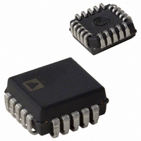
IC V-F CONV SYNCH MONO 5V 20PLCC
Manufacturer
Analog Devices Inc
Type
Voltage to Frequencyr
Datasheet
1.AD652JPZ.pdf
(28 pages)
Specifications of AD652JP
Rohs Status
RoHS non-compliant
Frequency - Max
2MHz
Full Scale
±25ppm/°C
Linearity
±0.005%
Mounting Type
Surface Mount
Package / Case
20-LCC (J-Lead)
Converter Function
VFC
Full Scale Frequency
2000
Power Supply Requirement
Single/Dual
Single Supply Voltage (max)
36V
Single Supply Voltage (min)
12V
Dual Supply Voltage (typ)
±15V
Dual Supply Voltage (min)
±6V
Dual Supply Voltage (max)
±18V
Operating Temperature (min)
0C
Operating Temperature (max)
70C
Operating Temperature Classification
Commercial
Package Type
PLCC
Lead Free Status / Rohs Status
Not Compliant
Available stocks
Company
Part Number
Manufacturer
Quantity
Price

Part Number:
AD652JP
Manufacturer:
ADI/亚德诺
Quantity:
20 000
Company:
Part Number:
AD652JP-REEL
Manufacturer:
Analog Devices Inc
Quantity:
10 000
Company:
Part Number:
AD652JP-REEL7
Manufacturer:
Analog Devices Inc
Quantity:
10 000
Part Number:
AD652JPZ
Manufacturer:
ADI/亚德诺
Quantity:
20 000


PLCC CONNECTIONS
The PLCC packaged AD652 offers additional input resistors not
found on the CERDIP-packaged device. These resistors provide
the user with additional input voltage ranges. Besides the 10 V
range available using the on-chip resistor in the CERDIP the
PLCC also offers 8 V and 5 V ranges. Figure 13A to Figure 13C
show the proper connections for these ranges with positive
input voltages. For negative input voltages, the appropriate
resistor should be tied to analog ground and the input voltage
should be applied to Pin 6, the + input of the op amp.
Bipolar input voltages can be accommodated by injecting
250 µA into Pin 5 with the use of the 5 V reference and the
input resistors. For the ±5 V or ±2.5 V range, the reference
output, Pin 20, should be tied to Pin 10. The input signal should
then be applied to Pin 8 for a ±5 V signal and to Pin 7 for a
±2.5 V signal. The input connections for a ±5 V range are
shown in Figure 13D. For a ±4 V range, the input signal should
be applied to Pin 9, and Pin 20 should be connected to Pin 8.
GAIN AND OFFSET CALIBRATION
The gain error of the AD652 is laser trimmed to within ±0.5%.
If higher accuracy is required, the internal 20 kΩ resistor must
be shunted with a 2 MΩ resistor to produce a parallel equivalent
that is 1% lower in value than the nominal 20 kΩ. Full-scale
adjustment is then accomplished using a 500 Ω series trimmer.
See Figure 14 and Figure 15. When negative input voltages are
used, this 500 Ω trimmer is tied to ground and Pin 6 is the
input pin.
+
–
V
IN
+
–
V
NC
NC
IN
5
6
7
8
5
6
7
8
A. PLCC 0V TO 10V INPUT
C. PLCC 0V TO 5V INPUT
10kΩ
10kΩ
10kΩ
10kΩ
NC
NC
9
9
16kΩ
16kΩ
NC
NC
10
10
SYNCHRONOUS
4kΩ
SYNCHRONOUS
4kΩ
VOLTAGE-TO-
VOLTAGE-TO-
FREQUENCY
CONVERTER
FREQUENCY
CONVERTER
AD652
AD652
Rev. C | Page 11 of 28
Figure 13.
NC
NC
NC
OFFSET
±
V
±
3.5mV
5V
V
IN
TRIM
5
6
7
8
5
6
7
8
IN
B. PLCC 0V TO 8V INPUT
V
10kΩ
10kΩ
10kΩ
10kΩ
250kΩ
IN
500Ω
D. PLCC
500Ω
0.02µF
500Ω
+V
+
–
NC
V
2MΩ
S
9
9
IN
16kΩ
16kΩ
±
5V INPUT
20kΩ
0.02µF
2MΩ
NC = NO CONNECT
20kΩ
NC
10
10
Figure 14. CERDIP Gain and Offset Trim
Figure 15. PLCC Gain and Offset Trim
4kΩ
4kΩ
SYNCHRONOUS
SYNCHRONOUS
350kΩ
VOLTAGE-TO-
VOLTAGE-TO-
FREQUENCY
CONVERTER
FREQUENCY
CONVERTER
AD652
AD652
1
2
3
4
5
6
7
8
5V REF
20kΩ
4
5
6
7
8
SYNCHRONOUS
20
VOLTAGE-TO-
FREQUENCY
CONVERTER
AD652
VOLTAGE-TO-FREQUENCY
10kΩ
10kΩ
16kΩ
1mA
SYNCHRONOUS
3
9
CONVERTER
AD652
10
2
1mA
4kΩ
REFERENCE
AND
5V
AND
11
1
D
SHOT
ONE
Q
Q
FLOP
SHOT
D
REFERENCE
ONE
20
12
"D"
CK
Q
Q
FLOP
5V
"D"
CK
AD652
19
13
16
15
14
13
12
11
10
9
18
17
16
15
14
Related parts for AD652JP
Image
Part Number
Description
Manufacturer
Datasheet
Request
R

Part Number:
Description:
±1.7g Dual-Axis IMEMS Accelerometer Evaluation Board
Manufacturer:
Analog Devices Inc
Datasheet:

Part Number:
Description:
Inertial Sensor Evaluation System
Manufacturer:
Analog Devices Inc
Datasheet:
Part Number:
Description:
Manufacturer:
Analog Devices Inc
Datasheet:
Part Number:
Description:
Manufacturer:
Analog Devices Inc
Datasheet:
Part Number:
Description:
Manufacturer:
Analog Devices Inc
Datasheet:
Part Number:
Description:
Manufacturer:
Analog Devices Inc
Datasheet:
Part Number:
Description:
Manufacturer:
Analog Devices Inc
Datasheet:
Part Number:
Description:
Manufacturer:
Analog Devices Inc
Datasheet:
Part Number:
Description:
Manufacturer:
Analog Devices Inc
Datasheet:
Part Number:
Description:
Manufacturer:
Analog Devices Inc
Datasheet:
Part Number:
Description:
Manufacturer:
Analog Devices Inc
Datasheet:
Part Number:
Description:
Manufacturer:
Analog Devices Inc
Datasheet:
Part Number:
Description:
Manufacturer:
Analog Devices Inc
Datasheet: