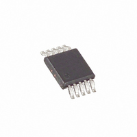
MAX6683AUB+T Maxim Integrated Products, MAX6683AUB+T Datasheet - Page 5

MAX6683AUB+T
Manufacturer Part Number
MAX6683AUB+T
Description
IC TEMP SENSOR MON 10-UMAX
Manufacturer
Maxim Integrated Products
Datasheet
1.MAX6683AUBT.pdf
(14 pages)
Specifications of MAX6683AUB+T
Function
Temp Monitoring System (Sensor)
Topology
ADC, Multiplexer, Register Bank
Sensor Type
Internal
Sensing Temperature
-40°C ~ 125°C
Output Type
I²C™/SMBus™
Output Alarm
Yes
Output Fan
No
Voltage - Supply
2.7 V ~ 5.5 V
Operating Temperature
-40°C ~ 125°C
Mounting Type
Surface Mount
Package / Case
10-MSOP, Micro10™, 10-uMAX, 10-uSOP
Full Temp Accuracy
+/- 3 C
Digital Output - Bus Interface
Serial (2-Wire)
Digital Output - Number Of Bits
10 bit + Sign
Maximum Operating Temperature
+ 125 C
Minimum Operating Temperature
- 40 C
Lead Free Status / RoHS Status
Lead free / RoHS Compliant
The MAX6683 is a voltage and temperature monitor
designed to communicate through an SMBus/I
face with an external microcontroller (µC). A µC with no
built-in I
serial commands by “bit-banging” general-purpose
input-output (GPIO) pins.
The MAX6683 can monitor external supply voltages of
typically 1.8V, 2.5V, 5V, as well as its own supply volt-
age and temperature. This makes it ideal for supervisor
and thermal management applications in telecommuni-
cations, desktop and notebook computers, worksta-
tions, and networking equipment. Voltage inputs are
converted to an 8-bit code and temperature is convert-
ed to an 11-bit code. The high-order 8 bits of the tem-
perature conversion can be read using a read byte
operation through the I
perature conversion is read using a read word opera-
tion and disregarding the lower 5 bits of the low byte.
By setting bit 5 of the Configuration Register to 1, the
temperature conversion can be reduced to 9 bits with a
four-fold reduction in conversion time. In this case, the
lower 7 bits of the low byte should be disregarded; 8-
bit temperature data has a resolution of 1°C/LSB, while
11-bit temperature data has a resolution of 0.125°C/
LSB. Setting bit 5 of the Configuration Register to 1
reduces the monitoring cycle time by a factor of 4. In
this case, a read word operation for temperature data
yields a 9-bit code in which the lower 7 bits of the low
byte should be disregarded. The LSB of the 9-bit tem-
perature data has a value of 0.5°C.
PIN
10
1
2
3
4
5
6
7
8
9
2
C or SMBus capabilities can generate SMBus
ALERT
NAME
1.8V
2.5V
GND
5V
N.C.
ADD
SDA
SCL
V
CC
IN
IN
IN
_______________________________________________________________________________________
Analog Input. Monitors 1.8V nominal supply.
Analog Input. Monitors 2.5V nominal supply.
Analog Input. Monitors 5V nominal supply.
No Connect. Not internally connected. Connect to GND to improve thermal conductivity.
Ground
SMBus Alert (Interrupt) Output, Open Drain. Alerts the master that a temperature or voltage limit has been
violated.
SMBus/I
transaction, and the 2LSBs of the Slave Address register are detemined by ADD’s connection to GND, SDA,
SCL, or V
SMBus/I
SMBus/I
Supply Voltage Input, +2.7V to +5.5V. Also serves as a voltage monitor input. Bypass V
0.1µF capacitor.
Detailed Description
2
C interface. The full 11-bit tem-
2
2
2
C-Compatible Address Select Input. ADD is sampled at the beginning of each SMBus/I
C-Compatible Serial Data Interface
C-Compatible Clock Input
CC
.
System Monitor in a 10-Pin µMAX
2
C inter-
Temperature Sensor and
Each input voltage is scaled down by an on-chip resis-
tive voltage-divider so that its output, at the nominal
input voltage, is 3/4 of the ADC’s full-scale range, or a
decimal count of 192 (Table 3). Input voltages other
than the nominal values may be used; ensure that they
fall within the usable ranges of pins to which they are
applied. Attenuate voltages greater than 6V with an
external resistive voltage-divider.
Writing a 1 to bit 0 of the Configuration Register starts
the monitoring function. The device performs a sequen-
tial sampling of all the inputs, starting with the internal
temperature sensor and continuing with 2.5V
5V
the sequential sampling does not stop until the sam-
pling cycle is completed and the results are stored.
When it starts again, it always starts with the tempera-
ture measurement.
An interrupt signal is generated when a temperature
measurement goes above the hot limit or when a volt-
age measurement is either above the high limit or
below the low limit. This causes the open-drain output
ALERT to go to the active-low state and set each corre-
sponding interrupt status bit (bits 0 through 4) to 1
(Table 5). The interrupt is cleared by reading the
Interrupt Status Register except for temperature inter-
rupts generated in comparator mode. Reading the
Interrupt Status Register also clears the register itself,
except for temperature interrupt bits set in comparator
mode.
FUNCTION
IN
, and V
CC
. If the master terminates the conversion,
Pin Description
CC
to GND with a
2
C
IN
, 1.8V
IN
5
,


