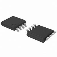
SE97PW,118 NXP Semiconductors, SE97PW,118 Datasheet - Page 31

SE97PW,118
Manufacturer Part Number
SE97PW,118
Description
IC TEMP SENSOR DIMM 8-TSSOP
Manufacturer
NXP Semiconductors
Datasheet
1.SE97TK118.pdf
(55 pages)
Specifications of SE97PW,118
Function
Temp Monitoring System (Sensor)
Topology
ADC (Sigma Delta), Comparator, Register Bank
Sensor Type
Internal
Sensing Temperature
-40°C ~ 125°C
Output Type
I²C™/SMBus™
Output Alarm
Yes
Output Fan
Yes
Voltage - Supply
3 V ~ 3.6 V
Operating Temperature
-40°C ~ 125°C
Mounting Type
Surface Mount
Package / Case
8-TSSOP
Temperature Threshold
+ 165 C
Full Temp Accuracy
1 %
Digital Output - Bus Interface
I2C, SMBus
Digital Output - Number Of Bits
11 bit
Supply Voltage (max)
3.6 V
Supply Voltage (min)
3 V
Description/function
Memory Module Temperature Sensor
Maximum Operating Temperature
+ 125 C
Minimum Operating Temperature
- 40 C
Supply Current
250 uA
Lead Free Status / RoHS Status
Lead free / RoHS Compliant
Other names
568-4291-2
935284062118
SE97PW-T
935284062118
SE97PW-T
NXP Semiconductors
SE97_7
Product data sheet
8.5.2 Lower Boundary Alarm Trip register (16-bit read/write)
8.5.3 Critical Alarm Trip register (16-bit read/write)
The value is the lower threshold temperature value for Alarm mode. The data format is
2’s complement with bit 2 = 0.25 °C. RFU bits will always report zero. Interrupts will
respond to the presently programmed boundary values. If boundary values are being
altered in-system, it is advised to turn off interrupts until a known state can be obtained to
avoid superfluous interrupt activity.
Table 17.
Table 18.
The value is the critical temperature. The data format is 2’s complement with
bit 2 = 0.25 °C. RFU bits will always report zero.
Table 19.
Table 20.
Bit
Symbol
Default
Access
Bit
15:13
12
11:2
1:0
Bit
Symbol
Default
Access
Bit
15:13
12
11:2
1:0
Bit
Symbol
Default
Access
Bit
Symbol
Default
Access
Symbol
RFU
SIGN
LBT
RFU
Symbol
RFU
SIGN
CT
RFU
Lower Boundary Alarm Trip register bit allocation
Lower Boundary Alarm Trip register bit description
Lower Boundary Alarm Trip register bit allocation
Critical Alarm Trip register bit description
R/W
R/W
15
15
R
R
0
0
7
0
7
0
Rev. 07 — 29 January 2010
RFU
RFU
R/W
R/W
14
14
DDR memory module temp sensor with integrated SPD, 3.3 V
R
R
0
0
6
0
6
0
Description
Sign (MSB)
reserved; always ‘0’
Description
Sign (MSB)
reserved; always ‘0’
reserved; always ‘0’
Lower Boundary Alarm Trip Temperature (LSB = 0.25 °C)
reserved; always ‘0’
Critical Alarm Trip Temperature (LSB = 0.25 °C)
R/W
R/W
13
13
R
R
0
0
5
0
5
0
LBT
CT
SIGN
SIGN
R/W
R/W
R/W
R/W
12
12
0
0
4
0
4
0
R/W
R/W
R/W
R/W
11
11
0
0
3
0
3
0
R/W
R/W
R/W
R/W
10
10
0
0
2
0
2
0
LBT
CT
© NXP B.V. 2010. All rights reserved.
R/W
R/W
9
0
R
9
0
R
1
0
1
0
RFU
RFU
SE97
R/W
R/W
31 of 55
8
0
R
8
0
R
0
0
0
0


