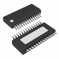
MAX8734AEEI+ Maxim Integrated Products, MAX8734AEEI+ Datasheet - Page 30

MAX8734AEEI+
Manufacturer Part Number
MAX8734AEEI+
Description
IC PWR SUPPLY CONTROLLER 28QSOP
Manufacturer
Maxim Integrated Products
Datasheet
1.MAX8734AEEIT.pdf
(33 pages)
Specifications of MAX8734AEEI+
Applications
Power Supply Controller
Voltage - Input
4.5 ~ 24 V
Current - Supply
25µA
Operating Temperature
-40°C ~ 85°C
Mounting Type
Surface Mount
Package / Case
28-QSOP
Product
Power Monitors
Operating Temperature Range
- 40 C to + 85 C
Mounting Style
SMD/SMT
Accuracy
1.5 %
Supply Current (max)
50 uA
Supply Voltage (max)
4.5 V
Supply Voltage (min)
24 V
Case
SSOP
Dc
06+
Lead Free Status / RoHS Status
Lead free / RoHS Compliant
Voltage - Supply
-
Lead Free Status / Rohs Status
Lead free / RoHS Compliant
High-Efficiency, Quad-Output, Main Power-
Supply Controllers for Notebook Computers
tion may be required on the secondary output to protect
any device connected to this output.
Careful PC board layout is critical to achieve minimal
switching losses and clean, stable operation. This is
especially true when multiple converters are on the
same PC board where one circuit can affect the other.
The switching power stages require particular attention
(Figure 13). Refer to the MAX1999 EV kit I.C. data sheet
for a specific layout example.
Mount all of the power components on the top side of
the board with their ground terminals flush against one
another, if possible. Follow these guidelines for good
PC board layout:
• Isolate the power components on the top side from
• Use a star ground connection on the power plane to
• Keep the high-current paths short, especially at the
• Keep the power traces and load connections short.
Figure 13. PC Board Layout Example
30
the sensitive analog components on the bottom side
with a ground shield. Use a separate PGND plane
under the OUT3 and OUT5 sides (called PGND3 and
PGND5). Avoid the introduction of AC currents into
the PGND3 and PGND5 ground planes. Run the
power plane ground currents on the top side only, if
possible.
minimize the crosstalk between OUT3 and OUT5.
ground terminals. This practice is essential for sta-
ble, jitter-free operation.
This practice is essential for high efficiency. Using
thick copper PC boards (2oz vs. 1oz) can enhance
______________________________________________________________________________________
ANALOG GROUND
PLANE ON INNER LAYER
USE AGND PLANE TO:
- BYPASS V
- TERMINATE EXTERNAL FB
- TERMINATE R
- PIN-STRAP CONTROL
INPUTS
DIVIDER (IF USED)
(IF USED)
CC
PC Board Layout Guidelines
CONNECT PGND TO AGND
BENEATH THE CONTROLLER AT
ONE POINT ONLY AS SHOWN.
AND REF
ILIM
AGND
USE PGND PLANE TO:
- BYPASS LDO_
- CONNECT PGND TO THE TOPSIDE STAR GROUND
AND ANALOG GROUND
VIA BETWEEN POWER
VIAS TO GROUND
PGND
NOTE: EXAMPLE SHOWN IS FOR DUAL I.C. n-CHANNEL MOSFET.
VIA TO OUT5
VIA TO LX5
OUT5
L1
C3
• CS_ (MAX8732A/MAX8733A)/LX_ (MAX8734A) and
• When trade-offs in trace lengths must be made, it is
• Ensure that the OUT_ connection to C
• Route high-speed switching nodes (BST_, DH_, LX_,
full-load efficiency by 1% or more. Correctly routing
PC board traces must be approached in terms of
fractions of centimeters, where a single milliohm of
excess trace resistance causes a measurable effi-
ciency penalty.
GND connections to the synchronous rectifiers for
current limiting must be made using Kelvin-sense
connections to guarantee the current-limit accuracy.
With 8-pin SO MOSFETs, this is best done by routing
power to the MOSFETs from outside using the top
copper layer, while connecting CS_/LX_ traces inside
(underneath) the MOSFETs.
preferable to allow the inductor charging path to be
made longer than the discharge path. For example, it
is better to allow some extra distance between the
input capacitors and the high-side MOSFET than to
allow distance between the inductor and the syn-
chronous rectifier or between the inductor and the
output filter capacitor.
direct. However, in some cases it may be desirable to
deliberately introduce some trace length between the
OUT_ connector node and the output filter capacitor
(see the Stability Considerations section).
and DL_) away from sensitive analog areas (REF,
ILIM_, and FB_). Use PGND3 and PGND5 as an EMI
shield to keep radiated switching noise away from the
IC’s feedback divider and analog bypass capacitors.
N4
N3
GROUND
C1
V+
C2
N1
N2
VIA TO LX3
VIA TO PGND
C4
OUT3
L2
VIA TO OUT3
OUT_
is short and


