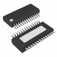
MAX8734AEEI+ Maxim Integrated Products, MAX8734AEEI+ Datasheet - Page 27

MAX8734AEEI+
Manufacturer Part Number
MAX8734AEEI+
Description
IC PWR SUPPLY CONTROLLER 28QSOP
Manufacturer
Maxim Integrated Products
Datasheet
1.MAX8734AEEIT.pdf
(33 pages)
Specifications of MAX8734AEEI+
Applications
Power Supply Controller
Voltage - Input
4.5 ~ 24 V
Current - Supply
25µA
Operating Temperature
-40°C ~ 85°C
Mounting Type
Surface Mount
Package / Case
28-QSOP
Product
Power Monitors
Operating Temperature Range
- 40 C to + 85 C
Mounting Style
SMD/SMT
Accuracy
1.5 %
Supply Current (max)
50 uA
Supply Voltage (max)
4.5 V
Supply Voltage (min)
24 V
Case
SSOP
Dc
06+
Lead Free Status / RoHS Status
Lead free / RoHS Compliant
Voltage - Supply
-
Lead Free Status / Rohs Status
Lead free / RoHS Compliant
The maximum input capacitor RMS current for a single
SMPS is given by:
When V+ = 2 x V
current of I
The ESR of the input capacitor is important for deter-
mining capacitor power dissipation. All the power
(I
ciency. Nontantalum chemistries (ceramic or OS-CON)
are preferred due to their low ESR and resilience to
power-up surge currents. Choose input capacitors that
exhibit less than +10°C temperature rise at the RMS
input current for optimal circuit longevity. Place the
drains of the high-side switches close to each other to
share common input bypass capacitors.
Most of the following MOSFET guidelines focus on the
challenge of obtaining high load-current capability
(> 5A) when using high-voltage (> 20V) AC adapters.
Low-current applications usually require less attention.
Choose a high-side MOSFET (N1/N3) that has conduc-
tion losses equal to the switching losses at the typical
battery voltage for maximum efficiency. Ensure that the
conduction losses at the minimum input voltage do not
exceed the package thermal limits or violate the overall
thermal budget. Ensure that conduction losses plus
switching losses at the maximum input voltage do not
exceed the package ratings or violate the overall ther-
mal budget.
Choose a synchronous rectifier (N2/N4) with the lowest
possible R
high-side switch turning on due to parasitic drain-to-gate
capacitance, causing crossconduction problems.
Switching losses are not an issue for the synchronous
rectifier in the buck topology since it is a zero-voltage
switched device when using the buck topology.
Worst-case conduction losses occur at the duty-factor
extremes. For the high-side MOSFET, the worst-case
power dissipation (PD) due to the MOSFET’s R
occurs at the minimum battery voltage:
RMS 2
PD N
(
H
x ESR) heats up the capacitor and reduces effi-
I
Re
RMS
DS(ON)
Supply Controllers for Notebook Computers
LOAD
sis
High-Efficiency, Quad-Output, Main Power-
≈
tan
I
/ 2.
. Ensure the gate is not pulled up by the
LOAD
OUT_
ce
______________________________________________________________________________________
MOSFET Power Dissipation
)
(D = 50%), I
=
Power-MOSFET Selection
V
OUT
V
V
IN MIN
OUT
(
_
(
V
_
V
)
+ −
+
RMS
(
I
V
LOAD
OUT
has a maximum
_
)
2
)
R
DS ON
DS(ON)
(
)
Generally, a small high-side MOSFET reduces switch-
ing losses at high input voltage. However, the R
required to stay within package power-dissipation limits
often limits how small the MOSFET can be. The opti-
mum situation occurs when the switching (AC) losses
equal the conduction (R
Switching losses in the high-side MOSFET can become
an insidious heat problem when maximum battery volt-
age is applied, due to the squared term in the CV
switching-loss equation. Reconsider the high-side
MOSFET chosen for adequate R
voltages if it becomes extraordinarily hot when subject-
ed to V+
Calculating the power dissipation in N
switching losses is difficult since it must allow for quan-
tifying factors that influence the turn-on and turn-off
times. These factors include the internal gate resis-
tance, gate charge, threshold voltage, source induc-
tance, and PC board layout characteristics. The
following switching-loss calculation provides only a
very rough estimate and is no substitute for bench eval-
uation, preferably including verification using a thermo-
couple mounted on N
where C
Q
the peak gate-drive source/sink current.
For the synchronous rectifier, the worst-case power dis-
sipation always occurs at maximum battery voltage:
The absolute worst case for MOSFET power dissipation
occurs under heavy overloads that are greater than
I
the current limit and cause the fault latch to trip. To pro-
tect against this possibility, “overdesign” the circuit to
tolerate:
where I
allowed by the current-limit circuit, including threshold
tolerance and resistance variation.
LOAD(MAX)
G(SW)
I
LOAD
PD N
is the switch gate charge of N
LIMIT(HIGH)
(MAX)
OSS
( )
= I
but are not quite high enough to exceed
L
is the output capacitance of N
.
LIMIT(HIGH)
V
=
C
IN MAX LOAD G SW SW
PD N Switching
1
OSS IN MAX
(
−
(
H
V
is the maximum valley current
(
V
IN MAX
H
V
)
(N1/N3):
I
OUT
DS(ON)
(
I
GATE
(
+ (LIR / 2 ) x I
2
_
)
Q
) losses.
)
)
2
I
(
LOAD
f
DS(ON)
SW
)
=
)
f
+
2
H
H
LOAD(MAX)
R
(N1/N3) due to
, and I
DS ON
at low battery
(
H
(N1/N3),
)
GATE
DS(ON)
2 ✕
27
is
f


