MAX8792ETD+T Maxim Integrated Products, MAX8792ETD+T Datasheet - Page 20

MAX8792ETD+T
Manufacturer Part Number
MAX8792ETD+T
Description
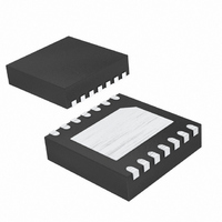
IC PWM CONTROLLER 14TDFN
Manufacturer
Maxim Integrated Products
Datasheet
1.MAX8792ETDT.pdf
(29 pages)
Specifications of MAX8792ETD+T
Applications
PWM Controller
Voltage - Input
2 ~ 26 V
Current - Supply
700µA
Operating Temperature
-40°C ~ 80°C
Mounting Type
Surface Mount
Package / Case
14-TDFN Exposed Pad
Lead Free Status / RoHS Status
Lead free / RoHS Compliant
Voltage - Supply
-
Lead Free Status / Rohs Status
Lead free / RoHS Compliant
Single Quick-PWM Step-Down
Controller with Dynamic REFIN
•
•
The switching frequency and operating point (% ripple
current or LIR) determine the inductor value as follows:
Find a low-loss inductor having the lowest possible DC
resistance that fits in the allotted dimensions. Ferrite
cores are often the best choice, although powdered
iron is inexpensive and can work well at 200kHz. The
core must be large enough not to saturate at the peak
inductor current (I
The inductor ripple current impacts transient-response
performance, especially at low V
Low inductor values allow the inductor current to slew
faster, replenishing charge removed from the output fil-
ter capacitors by a sudden load step. The amount of
output sag is also a function of the maximum duty factor,
20
capacitor selection, inductor saturation rating, and
the design of the current-limit circuit. The continu-
ous load current (I
stresses and thus drives the selection of input
capacitors, MOSFETs, and other critical heat-con-
tributing components. Most notebook loads gener-
ally exhibit I
Switching frequency: This choice determines the
basic trade-off between size and efficiency. The
optimal frequency is largely a function of maximum
input voltage due to MOSFET switching losses that
are proportional to frequency and V
mum frequency is also a moving target, due to
rapid improvements in MOSFET technology that are
making higher frequencies more practical.
Inductor operating point: This choice provides
trade-offs between size vs. efficiency and transient
response vs. output noise. Low inductor values pro-
vide better transient response and smaller physical
size, but also result in lower efficiency and higher
output noise due to increased ripple current. The
minimum practical inductor value is one that causes
the circuit to operate at the edge of critical conduc-
tion (where the inductor current just touches zero
with every cycle at maximum load). Inductor values
lower than this grant no further size-reduction bene-
fit. The optimum operating point is usually found
between 20% and 50% ripple current.
______________________________________________________________________________________
L
=
LOAD
⎛
⎜
⎝
I
PEAK
f
SW LOAD MAX
PEAK
I
V
IN
= I
=
):
I
LOAD MAX
LOAD
−
LOAD(MAX)
V
(
OUT
(
) determines the thermal
Transient Response
)
LIR
Inductor Selection
IN
)
⎞
⎟
⎠
+
x 80%.
⎛
⎜
⎝
- V
Δ
V
2
I
OUT
V
L
OUT
IN
IN
⎞
⎟
⎠
2
differentials.
. The opti-
which can be calculated from the on-time and minimum
off-time. The worst-case output sag voltage can be
determined by:
where t
Characteristics table).
The amount of overshoot due to stored inductor energy
when the load is removed can be calculated as:
The minimum current-limit threshold must be high
enough to support the maximum load current when the
current limit is at the minimum tolerance value. The val-
ley of the inductor current occurs at I
half the inductor ripple current (ΔIL); therefore:
where I
threshold voltage divided by the low-side MOSFETs on-
reistance (R
The valley current-limit threshold is precisely 1/20 the
voltage seen at ILIM. Connect a resistive divider from
REF to ILIM to analog ground (GND) in order to set a
fixed valley current-limit threshold. The external 400mV to
2V adjustment range corresponds to a 20mV to 100mV
valley current-limit threshold. When adjusting the current-
limit threshold, use 1% tolerance resistors and a divider
current of approximately 5µA to 10µA to prevent signifi-
cant inaccuracy in the valley current-limit tolerance.
The MAX8792 uses the low-side MOSFET’s on-resis-
tance as the current-sense element (R
R
the tolerance and thermal variation of the on-resistance.
Use the worst-case maximum value for R
the MOSFET data sheet, and add some margin for the
rise in R
to allow 0.5% additional resistance for each °C of tem-
perature rise, which must be included in the design
margin unless the design includes an NTC thermistor in
the ILIM resistive voltage-divider to thermally compen-
sate the current-limit threshold.
DS(ON)
V
SAG
OFF(MIN)
=
LIMIT(LOW)
DS(ON)
). Therefore, special attention must be made to
2
L I
C
(
DS(ON)
Δ
OUT OUT
I
LIMIT LOW
LOAD(MAX)
Setting the Valley Current Limit
V
with temperature. A good general rule is
is the minimum off-time (see the Electrical
SOAR
V
(
).
equals the minimum current-limit
⎡
⎢
⎢
⎣
≈
⎛
⎜
⎝
)
(
(
>
V
Δ
)
I
2
IN
LOAD MAX
I
2
LOAD MAX
C
⎡
⎢
⎣
−
⎛
⎜
⎝
OUT OUT
V
V
V
OUT SW
OUT SW
(
IN
(
V
V
IN
T
)
)
T
)
−
)
LOAD(MAX)
2
Δ
L
⎞
⎟ +
⎠
2
I
⎞
⎟ −
⎠
L
t
DS(ON)
OFF MIN
t
OFF MIN
SENSE
(
(
minus
from
)
)
⎤
⎥
⎦
⎤
⎥
⎥
⎦
=


