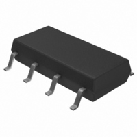
MB3771PF-G-BND-JNE1 Fujitsu Semiconductor America Inc, MB3771PF-G-BND-JNE1 Datasheet - Page 3

MB3771PF-G-BND-JNE1
Manufacturer Part Number
MB3771PF-G-BND-JNE1
Description
IC POWER SUPPLY MONITOR 8SOP
Manufacturer
Fujitsu Semiconductor America Inc
Datasheet
1.MB3771PF-G-BND-JNE1.pdf
(21 pages)
Specifications of MB3771PF-G-BND-JNE1
Applications
Power Supply Monitor
Voltage - Supply
3.5 V ~ 18 V
Current - Supply
350µA
Operating Temperature
-40°C ~ 85°C
Mounting Type
Surface Mount
Package / Case
8-SOP
Lead Free Status / RoHS Status
Lead free / RoHS Compliant
Voltage - Input
-
Other names
865-1021
Available stocks
Company
Part Number
Manufacturer
Quantity
Price
Company:
Part Number:
MB3771PF-G-BND-JNE1
Manufacturer:
Micrel
Quantity:
56
FUNCTIONAL DESCRIPTIONS
Comparators Comp.A and Comp.B apply a hysteresis to the detected voltage, so that when the voltage at either
the V
Comp. B may be used to detect any given voltage(Sample Application 3), and can also be used as a forced
reset pin (with reset hold time) with TTL input (Sample Application 6).
Note that if Comp.B is not used, the V
Instantaneous breaks or drops in the power supply can be detected as abnormal conditions by the MB3771
within a 2 s interval. However because momentary breaks or drops of this duration do not cause problems in
actual systems in some cases, a delayed trigger function can be created by connecting capacitors to the V
V
Because the RESET output has built-in pull-up resistance, there is no need to connect to external pull-up
resistance when connected to a high impedance load such as a CMOS logic IC.
Comparator Comp. C is an open-collector output comparator without hysteresis, in which the polarity of input/
output characteristics is reversed. Thus Comp. C is useful for over-voltage detection (Sample Application 11)
and positive logic RESET signal output (Sample Application 7), as well as for creating a reference voltage
(Sample Application 10).
Note that if Comp. C is not used, the V
FUNCTION EXPLANATION
(1) When V
(2) When V
(3) RESET goes high when CT begins charging.
(4) When V
(5) When V
In the case of voltage sagging, if the period from the time V
reaches V
successively.
(6) After T
(7) Same as Point 4.
(8) RESET remains low until V
V
T
C
SB
CC
T
PO
pin (Sample Application 8).
: = C
SA
or V
T
S
PO
CC
CC
CC
CC
+V
10
SB
passes, and V
1
2
3
4
rises to about 0.8V, RESET goes low.
reaches V
level dropps lower then V
level reaches V
pin falls below 1.23 V the RESET output signal goes to “low” level.
HYS
5
(Refer to C
again, is longer than t
7
6
5
8
S
+V
T
CC
HYS
pin capacitance vs. hold time )
S
level exceeds V
RESET
CC
+ V
, C
drops below 0.8V.
T
HYS
then begins charging. RESET remains low during this time
, then C
SB
SC
PI
RESET
S
, then RESET goes low and C
, (as specified in the AC Characteristics), C
pin should be connected to the V
pin should be connected to the GND pin (Sample Application 1).
V
CC
T
0.8 V
S
starts charging.
+ V
V
S
HYS
, then RESET goes high.
V
(1)
HYS
CC
(2)
goes lower than or equal to V
T
PO
(3)
T
starts discharging.
(4) (5) (6)
CC
pin (Sample Application 1).
T
PO
T
is discharged and charged
(7)
MB3771
(8)
S
to the time V
t
t
SA
or
CC
3


