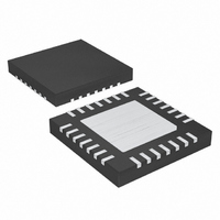
MAX17007GTI+ Maxim Integrated Products, MAX17007GTI+ Datasheet - Page 33

MAX17007GTI+
Manufacturer Part Number
MAX17007GTI+
Description
IC CTRLR QPWM GRAPHICS 28TQFN
Manufacturer
Maxim Integrated Products
Series
Quick-PWM™r
Datasheet
1.MAX17007AGTI.pdf
(35 pages)
Specifications of MAX17007GTI+
Applications
Power Supplies
Current - Supply
1.7mA
Voltage - Supply
4.5 V ~ 26 V
Operating Temperature
-40°C ~ 105°C
Mounting Type
Surface Mount
Package / Case
28-TQFN Exposed Pad
Lead Free Status / RoHS Status
Lead free / RoHS Compliant
In a single-phase configuration, the absolute point of
dropout is when the inductor current ramps down dur-
ing the minimum off-time (∆I
up during the on-time (∆I
∆I
current higher in response to increased load and must
always be greater than 1. As h approaches 1—the
absolute minimum dropout point—the inductor current
cannot increase as much during each switching cycle,
and V
capacitance is used. A reasonable minimum value for h
is 1.5, but adjusting this up or down allows trade-offs
between V
operating voltage. For a given value of h, the minimum
operating voltage can be calculated as:
where V
path (see the On-Time One-Shot section), and t
is from the Electrical Characteristics table. The absolute
minimum input voltage is calculated with h = 1.
If the calculated V
imum input voltage, then reduce the operating frequency
or add output capacitance to obtain an acceptable V
If operation near dropout is anticipated, calculate V
be sure of adequate transient response.
Dropout Design Example:
V
f
t
V
h = 1.5
Calculating again with h = 1 gives the absolute limit of
dropout:
Therefore, V
very large output capacitance, and a practical input volt-
age with reasonable output capacitance would be 2.0V.
SW
OFF(MIN)
OUT
CHG
DOWN
= 300kHz
V
V
= 1.5V
SAG
IN MIN
IN MIN
= 150mV (10A load)
(
(
CHG
is an indicator of the ability to slew the inductor
= 250ns
greatly increases unless additional output
V
SAG
)
)
IN
IN MIN
is the parasitic voltage drop in the charge
=
=
(
⎡
⎢
⎣
⎡
⎢
⎣
Core Controllers for Notebook Computers
must be greater than 1.78V, even with
, output capacitance, and minimum
1 0 25
1 0 25
IN(MIN)
−
−
______________________________________________________________________________________
)
( .
( .
=
⎛
⎜
⎜
⎝
1 5
1 5
1
.
.
−
µ
µ
Dual and Combinable QPWM Graphics
is greater than the required min-
V
s
V
s
(
V
h t
×
×
+
+
OUT
×
DOWN
1 5 300
1 0 300
150
150
UP
.
.
OFF MIN SW
). The ratio h = ∆I
×
×
−
mV
mV
V
(
) as much as it ramps
CHG
kHz
kHz
)
f
)
)
⎤
⎥ =
⎦
⎤
⎥ =
⎦
)
⎞
⎟
⎟
⎠
1 86
1 78
.
.
OFF(MIN)
V
V
SAG
SAG
UP
to
/
.
Careful PCB layout is critical to achieve low switching
losses and clean, stable operation. The switching
power stage requires particular attention. If possible,
mount all the power components on the top side of the
board with their ground terminals flush against one
another. Follow these guidelines for good PCB layout:
•
•
•
•
•
•
1) Place the power components first, with ground ter-
2) Mount the controller IC adjacent to the low-side
Keep the high-current paths short, especially at the
ground terminals. This is essential for stable, jitter-
free operation.
Connect all analog grounds to a separate solid
copper plane, which connects to the GND pin of
the Quick-PWM controller. This includes the V
bypass capacitor, REF bypass capacitors, REFIN1
components, and feedback compensation/dividers.
Keep the power traces and load connections short.
This is essential for high efficiency. The use of thick
copper PCBs (2oz vs. 1oz) can enhance full-load
efficiency by 1% or more. Correctly routing PCB
traces is a difficult task that must be approached in
terms of fractions of centimeters, where a single
mΩ of excess trace resistance causes a measur-
able efficiency penalty.
Keep the high current, gate-driver traces (DL, DH,
LX, and BST) short and wide to minimize trace
resistance and inductance. This is essential for
high-power MOSFETs that require low-impedance
gate drivers to avoid shoot-through currents.
When trade-offs in trace lengths must be made, it is
preferable to allow the inductor charging path to be
made longer than the discharge path. For example,
it is better to allow some extra distance between the
input capacitors and the high-side MOSFET than to
allow distance between the inductor and the low-
side MOSFET or between the inductor and the out-
put filter capacitor.
Route high-speed switching nodes away from sensi-
tive analog areas (REF, REFIN1, FB2, CSH, and CSL).
minals adjacent (low-side MOSFET source, C
C
ble, make all these connections on the top layer
with wide, copper-filled areas.
MOSFET. The DL gate traces must be short and
wide (50 mils to 100 mils wide if the MOSFET is 1in
from the controller IC).
OUT
, and anode of the low-side Schottky). If possi-
PCB Layout Guidelines
Layout Procedure
CC
IN
33
,


