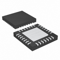
MAX17007GTI+ Maxim Integrated Products, MAX17007GTI+ Datasheet - Page 31

MAX17007GTI+
Manufacturer Part Number
MAX17007GTI+
Description
IC CTRLR QPWM GRAPHICS 28TQFN
Manufacturer
Maxim Integrated Products
Series
Quick-PWM™r
Datasheet
1.MAX17007AGTI.pdf
(35 pages)
Specifications of MAX17007GTI+
Applications
Power Supplies
Current - Supply
1.7mA
Voltage - Supply
4.5 V ~ 26 V
Operating Temperature
-40°C ~ 105°C
Mounting Type
Surface Mount
Package / Case
28-TQFN Exposed Pad
Lead Free Status / RoHS Status
Lead free / RoHS Compliant
When only using ceramic output capacitors, output
overshoot (V
output capacitance requirement. Their relatively low
capacitance value can allow significant output over-
shoot when stepping from full-load to no-load condi-
tions, unless designed with a small inductance value
and high switching frequency to minimize the energy
transferred from the inductor to the capacitor during
load-step recovery.
Unstable operation manifests itself in two related but
distinctly different ways: double pulsing and feedback
loop instability. Double pulsing occurs due to noise on
the output or because the ESR is so low that there is
not enough voltage ramp in the output voltage signal.
This “fools” the error comparator into triggering a new
cycle immediately after the minimum off-time period
has expired. Double pulsing is more annoying than
harmful, resulting in nothing worse than increased out-
put ripple. However, it can indicate the possible pres-
ence of loop instability due to insufficient ESR. Loop
instability can result in oscillations at the output after
line or load steps. Such perturbations are usually
damped, but can cause the output voltage to rise
above or fall below the tolerance limits.
The easiest method for checking stability is to apply a
very fast zero-to-max load transient and carefully
observe the output voltage ripple envelope for over-
shoot and ringing. It can help to simultaneously monitor
the inductor current with an AC current probe. Do not
allow more than one cycle of ringing after the initial
step-response under/overshoot.
The input capacitor must meet the ripple current
requirement (I
The I
lowing equation for a single-phase application:
In combined mode, the input RMS current simplifies to:
where I
phases.
For most applications, nontantalum chemistries (ceram-
ic, aluminum, or OS-CON) are preferred due to their
resistance to inrush surge currents typical of systems
with a mechanical switch or connector in series with the
I
RMS
RMS
=
LOAD
I
LOAD
I
RMS
requirements can be determined by the fol-
1
SOAR
2
RMS
is the combined output current of both
V
=
Core Controllers for Notebook Computers
OUT
⎛
⎜
⎝
I
LOAD
______________________________________________________________________________________
) imposed by the switching currents.
) typically determines the minimum
2
1
(
V
V
IN
IN
Input Capacitor Selection
−
⎞
⎟
⎠
Dual and Combinable QPWM Graphics
V
OUT
2
V
1
OUT IN
)
V
+
IN
I
LOAD
(
V
2
2
−
V
OUT
V
OUT
2
(
V
)
IN
−
V
OUT
2
)
input. If the Quick-PWM controller is operated as the
second stage of a two-stage power-conversion system,
tantalum input capacitors are acceptable. In either con-
figuration, choose an input capacitor that exhibits less
than +10°C temperature rise at the RMS input current
for optimal circuit longevity.
Most of the following MOSFET guidelines focus on the
challenge of obtaining high load-current capability
when using high-voltage (> 20V) AC adapters. Low-
current applications usually require less attention.
The high-side MOSFET (N
the resistive losses plus the switching losses at both
V
Ideally, the losses at V
losses at V
losses at V
at V
R
es at V
V
R
wide range, the minimum power dissipation occurs
where the resistive losses equal the switching losses.
Choose a low-side MOSFET that has the lowest possible
on-resistance (R
package (i.e., one or two 8-pin SOs, DPAK, or D
and is reasonably priced. Make sure that the DL gate
driver can supply sufficient current to support the gate
charge and the current injected into the parasitic gate-
to-drain capacitor caused by the high-side MOSFET
turning on; otherwise, cross-conduction problems might
occur (see the MOSFET Gate Drivers (DH, DL) section).
Worst-case conduction losses occur at the duty factor
extremes. For the high-side MOSFET (N
case power dissipation due to resistance occurs at the
minimum input voltage:
Generally, a small high-side MOSFET is desired to
reduce switching losses at high input voltages.
However, the R
power dissipation often limits how small the MOSFET
can be. Again, the optimum occurs when the switching
losses equal the conduction (R
side switching losses do not usually become an issue
until the input is greater than approximately 15V.
IN(MIN)
IN(MIN)
DS(ON)
DS(ON)
IN(MAX)
PD NH
IN(MAX)
(
, consider reducing the size of N
but with higher C
and V
to lower C
IN(MIN)
, consider increasing the size of N
IN(MAX)
Re
sistive
are significantly higher than the losses at
IN(MAX)
DS(ON)
DS(ON)
are significantly higher than the losses
, with lower losses in between. If the
GATE
)
=
IN(MIN)
Power-MOSFET Selection
. Calculate both of these sums.
⎛
⎜
⎝
required to stay within package
), comes in a moderate-sized
V
). If V
IN MIN
V
GATE
MOSFET Power Dissipation
H
OUT
(
) must be able to dissipate
should be roughly equal to
). Conversely, if the loss-
IN
)
⎞
⎟
⎠
DS(ON)
(
does not vary over a
I
LOAD
)
) losses. High-
2
H
R
H
), the worst-
DS ON
H
(increasing
(reducing
(
2
)
PAK),
31


