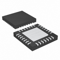
MAX17007GTI+ Maxim Integrated Products, MAX17007GTI+ Datasheet - Page 19

MAX17007GTI+
Manufacturer Part Number
MAX17007GTI+
Description
IC CTRLR QPWM GRAPHICS 28TQFN
Manufacturer
Maxim Integrated Products
Series
Quick-PWM™r
Datasheet
1.MAX17007AGTI.pdf
(35 pages)
Specifications of MAX17007GTI+
Applications
Power Supplies
Current - Supply
1.7mA
Voltage - Supply
4.5 V ~ 26 V
Operating Temperature
-40°C ~ 105°C
Mounting Type
Surface Mount
Package / Case
28-TQFN Exposed Pad
Lead Free Status / RoHS Status
Lead free / RoHS Compliant
Figure 4. PWM Controller Block Diagram
The Quick-PWM control architecture is a pseudo-fixed-
frequency, constant-on-time, current-mode regulator
with voltage feed-forward. This architecture relies on
the output filter capacitor’s ESR to act as a current-
sense resistor, so the output ripple voltage provides the
PWM ramp signal. The control algorithm is simple: the
high-side switch on-time is determined solely by a one-
shot whose pulse width is inversely proportional to
input voltage and directly proportional to output volt-
age. Another one-shot sets a minimum off-time (150ns
typ). The on-time one-shot is triggered if the error com-
parator is low, the low-side switch current is below the
valley current-limit threshold, and the minimum off-time
one-shot has timed out. Figure 4 is the PWM controller
block diagram.
TON
Free-Running Constant-On-Time PWM
TRIG
ONE-SHOT
Controller with Input Feed-Forward
t
ON
SMPS Detailed Description
Core Controllers for Notebook Computers
COMPUTE
Q
ON-TIME
SLOPE
COMP
______________________________________________________________________________________
AMPLIFIER
AMPLIFIED
CURRENT
ERROR
SENSE
Dual and Combinable QPWM Graphics
CSL OR
CCI
INTERNAL
FB
INTEGRATOR
(CCV)
TARGET
CURRENT
VALLEY
LIMIT
The heart of the PWM core is the one-shot that sets the
high-side switch on-time. This fast, low-jitter, adjustable
one-shot includes circuitry that varies the on-time in
response to battery and output voltage. In independent
mode, the high-side switch on-time is inversely propor-
tional to the battery voltage as sensed by the TON1
and TON2 inputs, and proportional to the voltages on
CSL1 and CSL2 pins:
where T
resistance between TON1 and V
resistance between TON2 and V
results in a nearly constant switching frequency despite
the lack of a fixed-frequency clock generator.
CROSSING
SMPS1 On-Time t
SMPS2 On-Time t
Q
SW1
ZERO
t
OFF(MIN)
(switching period of SMPS1) is set by the
TRIG
S
R
S
R
Q
Q
ON1
ON2
FAULT
= T
= T
OV
On-Time One-Shot
SW1
SW2
IN
, T
MAX17007
MAX17008
IN
(V
(V
SW2
. This algorithm
CSL1
CSL2
is set by the
/V
/V
DH DRIVER
IN
IN
DL DRIVER
)
)
19


