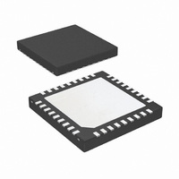
LP5551SQX/NOPB National Semiconductor, LP5551SQX/NOPB Datasheet - Page 9

LP5551SQX/NOPB
Manufacturer Part Number
LP5551SQX/NOPB
Description
IC ENERGY MGMNT SYSTEM 36-LLP
Manufacturer
National Semiconductor
Series
PowerWise®r
Datasheet
1.LP5551SQXNOPB.pdf
(32 pages)
Specifications of LP5551SQX/NOPB
Applications
Handheld/Mobile Devices
Current - Supply
431µA
Voltage - Supply
2.7 V ~ 5.5 V
Operating Temperature
-40°C ~ 85°C
Mounting Type
Surface Mount
Package / Case
36-LLP
For Use With
LP5551SQEV - BOARD EVALUATION LP5551SQ
Lead Free Status / RoHS Status
Lead free / RoHS Compliant
Other names
LP5551SQX
N-Well Bias Characteristics
values and limits appearing in normal type apply for TJ = 25°C. Limits appearing in boldface type apply over the entire junction
temperature range for operation, -40 to +125°C. (Notes 2, 7, 8)
P-Well Characteristics
and limits appearing in normal type apply for TJ = 25°C. Limits appearing in boldface type apply over the entire junction temperature
range for operation, -40 to +125°C. (Notes 2, 7, 8)
Symbol
V
Accuracy
V
Range
I
I
I
I
C
Symbol
V
Accuracy
V
I
Q
SOURCE/SINK
SC (SOURCE)
SC (SINK)
Q
OFFSET
OFFSET
OUT
OUT
LOAD
Range
Parameter
Output Voltage Offset Tolerance
Line Regulation
Load Regulation
Programmable Output Voltage
Offset: Referenced to V
Quiescent Current
Output Sourcing and Sinking
Capability
Output Source Short Circuit Limit V
Output Sink Short Circuit Limit
Output Capacitance Of Load
Parameter
Output Voltage Tolerance
Line Regulation
Load Regulation
Programmable Output Voltage
Offset:
Referenced to Ground
Quiescent Current
AVS
Unless otherwise noted, V
Unless otherwise noted, V
Conditions
V
V
Iout = 10 µA
2.7
I
2.7 V
V
VAVS = 1.2 V
0.1 uA
Programming Resolution: See
Register Table
V
V
V
Steady State
V
Steady State
V
V
Steady State
0 µA
OUT
Conditions
V
I
2.7
Bias Current Control bits = 00
I
V
2.7V
V
V
0.1 uA
0 mA
Programming Resolution: See
Register Table
IOUT = 0, P-well Bias Current Control
bits = 00
AVS
OFFSET
DD_A, _D
DD_A, _D
OFFSET
OFFSET
DD_A, _D
NWELL
DD_A, _D
NWELL
OUT
OUT
OUT
OUT
DD_A, _D
OUT
≤
= 10 uA,V
≤
≤
= 1.2 V
≤
= 10 µA
= 10 uA
V
≤
I
= 0 V
= 0.3 V
= 0.3 V
≤
V
≤
DD_A, _D
OUT
= 0 V
= V
V
≤
= -0.3 V
= 1 V
> V
DD_A, _D
V
, P
, P
, P
, P
IOUT
I
DD_A, _D
OUT
, P
DD_A, _D
I
DD_A
OUT
≤
VDD1,2
VDD1,2
VDD1,2
VDD1,2
OFFSET(NOM)
VDD1,2
9
3 uA
≤
OFFSET
, P
≤
≤
DD_A, _D
, P
10 uA
, P
10 uA
VDD1,2
10 uA
, P
= 3.6 V
= 3.6 V,
= 3.6 V,
= 3.6 V,
VDD1,2
= 3.6 V
VDD1,2
VDD1,2
= -0.315
, V
≤
- 15 mV
DD_A, _D
≤
≤
PVDD1,2
5.5 V
≤
5.5 V
5.5 V
5.5 V
, V
, RESETN, ENABLE = 3.6V. Typical values
PVDD1,2
Min
-0.363 -0.3
-0.315 0
3
0.1
Min
-0.035
-1
, RESETN, ENABLE = 3.6V. Typical
Typ
0.321
-0.107
50
1
Typ
0
0.159
0.011
0
150
Max
-0.266
1
42
65
5
Max
0.035
0.3
270
www.national.com
Units
V
%/V
%/µA
V
uA
Units
V
%/V
%/mA
V
uA
mA
mA
mA
nF


