LP5551SQX/NOPB National Semiconductor, LP5551SQX/NOPB Datasheet - Page 10
LP5551SQX/NOPB
Manufacturer Part Number
LP5551SQX/NOPB
Description
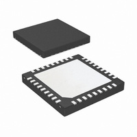
IC ENERGY MGMNT SYSTEM 36-LLP
Manufacturer
National Semiconductor
Series
PowerWise®r
Datasheet
1.LP5551SQXNOPB.pdf
(32 pages)
Specifications of LP5551SQX/NOPB
Applications
Handheld/Mobile Devices
Current - Supply
431µA
Voltage - Supply
2.7 V ~ 5.5 V
Operating Temperature
-40°C ~ 85°C
Mounting Type
Surface Mount
Package / Case
36-LLP
For Use With
LP5551SQEV - BOARD EVALUATION LP5551SQ
Lead Free Status / RoHS Status
Lead free / RoHS Compliant
Other names
LP5551SQX


www.national.com
Logic and Control Inputs
and limits appearing in normal type apply for TJ = 25°C. Limits appearing in boldface type apply over the entire junction temperature
range for operation, -40 to +125°C. (Notes 2, 7, 8, 9)
Logic and Control Outputs
values and limits appearing in normal type apply for TJ = 25°C. Limits appearing in boldface type apply over the entire junction
temperature range for operation, -40 to +125°C. (Notes 2, 7, 8, 9)
Note 1: Absolute Maximum Ratings indicate limits beyond which damage to the component may occur. Operating Ratings are conditions under which operation
of the device is guaranteed. Operating Ratings do not imply guaranteed performance limits. For guaranteed performance limits and associated test conditions,
see the Electrical Characteristics tables.
Note 2: All voltages are with respect to the potential at the GND pin.
Note 3: The Human body model is a 100 pF capacitor discharged through a 1.5 kΩ resistor into each pin.
The amount of Absolute Maximum power dissipation allowed for the device depends on the ambient temperature and can be calculated using the formula P =
(TJ – TA)/θ
Junction-to-ambient thermal resistance is highly application and board-layout dependent. In applications where high maximum power dissipation exists, special
care must be paid to thermal dissipation issues in board design.
Internal thermal shutdown circuitry protects the device from permanent damage. Thermal shutdown engages at TJ=150°C (typ.) and disengages at TJ=140°C
(typ.).
Symbol
I
I
C
Symbol
PWI
V
V
V
I
I
R
T
Symbol
V
V
V
SINK
SOURCE
IL
IL_PWI
EN_LOW
LOAD
IL
IH
IH_PWI
PD_PWI
OL
OH
OH_PWI
CLOCK
JA
, (1) where TJ is the junction temperature, TA is the ambient temperature, and JA is the junction-to-ambient thermal resistance.
Parameter
Output Sinking Capability
Output Source Capability
Output Capacitance of Load
Parameter
Output low level
Output high level
Output high level, PWI
Parameter
Rated frequency
Input Low Level
Input High Level
Input High Level, PWI
Logic Input Current
Logic Input Current, PWI
Pull-down resistance for PWI
signals
Minimum low pulse width to
enter STARTUP state
Unless otherwise noted, V
Unless otherwise noted, V
Conditions
PWROK, GPOx, SPWI,
I
PWROK, GPOx, I
SPWI, I
Conditions
2.7 V
ENABLE, RESETN, SPWI, SCLK 2.7
V
ENABLE, RESETN 2.7 V
V
SPWI, SCLK, 1.5 V
ENABLE, RESETN, 0 V
V
SPWI, SCLK, 1.5 V
ENABLE pulsed high - low - high
SINK
PVDD1,2
PVDD1,2
Conditions
V
Bias Current Control bits = 00
V
V
Bias Current Control bits = 01
V
V
Bias Current Control bits = 10
V
V
Bias Current Control bits = 11
V
V
0µA
≤
DD_A, _D
OUT
DD_A, _D
OUT
DD_A, _D
OUT
DD_A, _D
OUT
DD_A, _D
V
≤
≤
DD_A, _D
≤
1 mA
SOURCE
> V
> V
> V
> V
V
I
≤
≤
OUT
DD_A, _D
, P
, P
, P
, P
, P
OUT(NOM)
OUT(NOM)
OUT(NOM)
OUT(NOM)
5.5 V
5.5 V
, V
≤
10
VDD1,2
VDD1,2
VDD1,2
VDD1,2
VDD1,2
≤
3 uA
PVDD1,2
, V
1 mA
SOURCE
DD_A, _D
PVDD1,2
= 3.6 V
= 3.6 V
= 3.6 V
= 3.6 V
= 2.7 V
≤
≤
- 15 mV(Note 12)
- 15 mV(Note 12)
- 15 mV(Note 12)
- 15 mV(Note 12)
V
V
O2
≤
O2
DD_A, _D
≤
≤
5.5 V
≤
≤
≤
, V
V
≤
1 mA V
V
3.3 V
DD_A, _D
3.3 V
PVDD1,2
5.5 V
DD_A, _D
, V
PVDD1,2
V
,
BAT1
, RESETN, ENABLE = 3.6V. Typical values
,
O2
Min
-0.4V
V
-0.4V
O2
Min
8
36
52
80
100
0.1
, RESETN, ENABLE = 3.6V. Typical
Min
0.5
-5
-5
-0.4V
2
Typ
Typ
1
Typ
10
1
Max
5
Max
0.4
Max
0.4
15
15
5
2
Units
uA
uA
nF
Units
V
V
V
Units
MHz
V
V
V
µA
µA
MΩ
µsec
Related parts for LP5551SQX/NOPB
Image
Part Number
Description
Manufacturer
Datasheet
Request
R

Part Number:
Description:
IC,Multiple Regulator Circuit,LLCC,36PIN,PLASTIC
Manufacturer:
National Semiconductor

Part Number:
Description:
IC ENERGY MANAGEMENT UNIT 36-LLP
Manufacturer:
National Semiconductor
Datasheet:
Part Number:
Description:
IC,Multiple Regulator Circuit,LLCC,36PIN,PLASTIC
Manufacturer:
National Semiconductor
Part Number:
Description:
National Semiconductor [8-Bit D/A Converter]
Manufacturer:
National Semiconductor
Datasheet:
Part Number:
Description:
National Semiconductor [Media Coprocessor]
Manufacturer:
National Semiconductor
Datasheet:
Part Number:
Description:
Digitally Controlled Tone and Volume Circuit with Stereo Audio Power Amplifier, Microphone Preamp Stage and National 3D Sound
Manufacturer:
National Semiconductor
Datasheet:
Part Number:
Description:
Digitally Controlled Tone and Volume Circuit with Stereo Audio Power Amplifier, Microphone Preamp Stage and National 3D Sound
Manufacturer:
National Semiconductor
Datasheet:
Part Number:
Description:
AC97 Rev 2 Codec with Sample Rate Conversion and National 3D Sound
Manufacturer:
National Semiconductor
Part Number:
Description:
Manufacturer:
National Semiconductor
Datasheet:
Part Number:
Description:
Manufacturer:
National Semiconductor
Datasheet:
Part Number:
Description:
General Purpose, Low Voltage, Low Power, Rail-to-Rail Output Operational Amplifiers
Manufacturer:
National Semiconductor
Datasheet:
Part Number:
Description:
8-bit 20 MSPS flash A/D converter.
Manufacturer:
National Semiconductor
Datasheet:
Part Number:
Description:
Low Noise Quad Operational Amplifier
Manufacturer:
National Semiconductor
Datasheet:
Part Number:
Description:
Quad Differential Line Receivers
Manufacturer:
National Semiconductor
Datasheet: