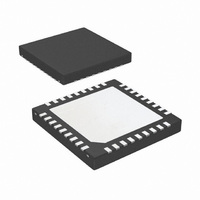
LP5551SQX/NOPB National Semiconductor, LP5551SQX/NOPB Datasheet - Page 25

LP5551SQX/NOPB
Manufacturer Part Number
LP5551SQX/NOPB
Description
IC ENERGY MGMNT SYSTEM 36-LLP
Manufacturer
National Semiconductor
Series
PowerWise®r
Datasheet
1.LP5551SQXNOPB.pdf
(32 pages)
Specifications of LP5551SQX/NOPB
Applications
Handheld/Mobile Devices
Current - Supply
431µA
Voltage - Supply
2.7 V ~ 5.5 V
Operating Temperature
-40°C ~ 85°C
Mounting Type
Surface Mount
Package / Case
36-LLP
For Use With
LP5551SQEV - BOARD EVALUATION LP5551SQ
Lead Free Status / RoHS Status
Lead free / RoHS Compliant
Other names
LP5551SQX
Operation Description
DEVICE INFORMATION
The LP5551 is a PowerWise Interface (PWI) compliant power
management unit (PMU) for application or baseband proces-
sors in mobile phones or other portable equipment. It oper-
ates
Semiconductor’s Advanced Power Controller (APC) to pro-
vide Adaptive or Dynamic Voltage Scaling (AVS, DVS) which
drastically improves processor efficiencies compared to con-
ventional power delivery methods. The LP5551 consists of a
high efficiency switching DC/DC buck converter to supply the
AVS or DVS voltage domain, three LDOs for supplying the
logic, PLL, and memory, and PWI registers and logic.
OPERATION STATE DIAGRAM
The LP5551 has four operating states: Start-up, Active, Sleep
and Standby.
The Start-up state is the default state after reset. All regulators
are off and PWROK output is ‘0’. The device will power up
when the external enable-input is pulled high. After the power-
up sequence LP5551 enters the Active state.
In the Active state all regulators are on and PWROK-output
is ‘1’. Immediately after Start-up the output voltages are at
cooperatively
with
processors
using
FIGURE 6. LP5551 State Diagram
National
25
their default levels. LP5551 can be turned off by supplying the
Shutdown command over PWI, or by setting ENABLE and/or
RESETN to '0'. The LP5551 can be switched to the Sleep
state by issuing the Sleep command.
In the Sleep state the core voltage regulator is off, but the
PWROK output is still ‘1’. The memory voltage regulator
(VO3) provides the programmed memory retention voltage.
LDO1 and LDO2 are on. The LP5551 can be activated from
the Sleep state by giving the Wake-up command. This re-
sumes the last programmed Active state configuration. The
device can also be switched off by giving the Shutdown com-
mand, or by setting ENABLE and/or RESETN to ‘0’
In the Shutdown-state all output voltages are ‘0’, and
PWROK-signal is ‘0’ as well. The LP5551 can exit the Shut-
down-state if either ENABLE or RESETN is ‘0’. In either case
the device moves to the Start-up state. See Figure 8.
Figure 6 shows the LP5551 state diagram. The figure as-
sumes that supply voltage to the regulator IC is in the valid
range.
20172145
www.national.com


