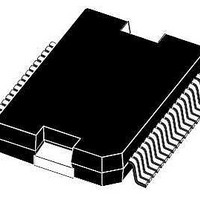
L9953 STMicroelectronics, L9953 Datasheet - Page 6

L9953
Manufacturer Part Number
L9953
Description
IC DVR DOOR ACTUATOR POWERSO-36
Manufacturer
STMicroelectronics
Datasheet
1.L9953XPTR.pdf
(38 pages)
Specifications of L9953
Applications
Door Actuator
Current - Supply
7mA
Voltage - Supply
7 V ~ 28 V
Operating Temperature
-40°C ~ 150°C
Mounting Type
Surface Mount
Package / Case
PowerSO-36 Exposed Bottom Pad
Mounting Style
SMD/SMT
Lead Free Status / RoHS Status
Lead free / RoHS Compliant
Available stocks
Company
Part Number
Manufacturer
Quantity
Price
Part Number:
L9953EXP
Manufacturer:
ST
Quantity:
20 000
Part Number:
L9953LXP
Manufacturer:
ST
Quantity:
20 000
Part Number:
L9953LXPTR
Manufacturer:
ST
Quantity:
20 000
Part Number:
L9953XP
Manufacturer:
ST
Quantity:
20 000
Company:
Part Number:
L9953XPTR
Manufacturer:
st
Quantity:
1 699
Part Number:
L9953XPTR
Manufacturer:
ST
Quantity:
20 000
Block diagram and pin description
1
6/38
Block diagram and pin description
Figure 1.
Table 2.
V C C
1, 18, 19, 36
** N o te : R e sisto rs b e tw e e n µ C a n d L 9 9 5 3 a re re co m m e n d e d to lim it c u rre n ts
fo r n e g a tiv e vo lta g e tra n sie n ts a t V B A T (e .g . IS O typ e 1 p u lse )
2, 35
Pin
3
4
5
µ C
V
B AT
Block diagram
Pin definitions and functions
R ev e rs e P olarit y
P rotec tion
**
**
**
**
**
Symbol
OUT8
OUT1
OUT2
OUT3
**
1k
1k
1k
1k
1k
GND
1k
P W M 2 / C M
100µ F
P W M 1
*
C L K
C S N
D O
D I
Ground:
Reference potential
Important: for the capability of driving the full current at the outputs all
pins of GND must be externally connected.
Highside driver output 8
The output is built by a highside switch and is intended for resistive
loads, hence the internal reverse diode from GND to the output is
missing. For ESD reason a diode to GND is present but the energy
which can be dissipated is limited. The highside driver is a power
DMOS transistor with an internal parasitic reverse diode from the
output to VS (bulk-drain-diode). The output is over-current and open
load protected.
Important: for the capability of driving the full current at the outputs both
pins of OUT8 must be externally connected.
Half-bridge-output 1,2,3
The output is built by a highside and a lowside switch, which are
internally connected. The output stage of both switches is a power
DMOS transistor. Each driver has an internal parasitic reverse diode
(bulk-drain-diode: highside driver from output to VS, lowside driver from
GND to output). This output is over-current and open load protected.
V C C
Doc ID 14278 Rev 3
V S
C h a rg e
P u m p
* N o te : V a lu e o f ca p a cito r h a s to b e ch o o s e n ca re fu lly to lim it th e V S vo lta g e b e lo w a b s o lu te
m a xim u m ra tin g s in c a se o f a n u n e xp e cte d fre e w h e e lin g co n d itio n (e .g . TS D , P O R )
M U X
G N D
4
Function
O U T 1
O U T 2
O U T 3
O U T 4
O U T 5
O U T 6
O U T 7
O U T 8
M
M
M
L9953 / L9953XP
M irro r C o m m o n
M irro r V e rtic a l
M irro r H o riz o n ta l
L o c k / F o ld e r
D e fro s te r


