L9951 STMicroelectronics, L9951 Datasheet - Page 22
L9951
Manufacturer Part Number
L9951
Description
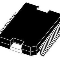
IC REAR DOOR ACT DVR POWERSO-36
Manufacturer
STMicroelectronics
Type
DC Motor Driverr
Datasheet
1.L9951XPTR.pdf
(36 pages)
Specifications of L9951
Applications
Automotive
Current - Supply
7mA
Voltage - Supply
7 V ~ 28 V
Operating Temperature
-40°C ~ 150°C
Mounting Type
Surface Mount
Package / Case
PowerSO-36 Exposed Bottom Pad
Operating Current
20mA
Operating Temperature Classification
Automotive
Motor Controller Type
DC Motor Driver
Package Type
PowerSO
Operating Supply Voltage (min)
7V
Operating Supply Voltage (max)
28V
Supply Current
20 mA
Mounting Style
SMD/SMT
Lead Free Status / RoHS Status
Lead free / RoHS Compliant
Available stocks
Company
Part Number
Manufacturer
Quantity
Price

Part Number:
L9951
Manufacturer:
ST
Quantity:
20 000
Part Number:
L9951XP
Manufacturer:
ST
Quantity:
20 000
Company:
Part Number:
L9951XPTR
Manufacturer:
st
Quantity:
6 966
Part Number:
L9951XPTR
Manufacturer:
ST
Quantity:
20 000


Functional description of the SPI
4
4.1
Note:
4.2
4.3
Note:
22/36
Functional description of the SPI
Serial Peripheral Interface (SPI)
This device uses a standard SPI to communicate with a microcontroller. The SPI can be
driven by a microcontroller with its SPI peripheral running in following mode: CPOL = 0 and
CPHA = 0.
For this mode, input data is sampled by the low to high transition of the clock CLK, and
output data is changed from the high to low transition of CLK.
This device is not limited to microcontroller with a build-in SPI. Only three CMOS-compatible
output pins and one input pin will be needed to communicate with the device. A fault
condition can be detected by setting CSN to low. If CSN = 0, the DO-pin will reflect the
status bit 0 (fault condition) of the device which is a logical-or of all bits in the status registers
0 and 1. The microcontroller can poll the status of the device without the need of a full SPI-
communication cycle.
In contrast to the SPI-standard the least significant bit (LSB) will be transferred first (see
Figure
Chip Select Not (CSN)
The input pin is used to select the serial interface of this device. When CSN is high, the
output pin (DO) will be in high impedance state. A low signal will activate the output driver
and a serial communication can be started.
The state when CSN is going low until the rising edge of CSN will be called a
communication frame. If the CSN-input pin is driven above 7.5V, the L9951 will go into a test
mode. In the test mode the DO will go from tristate to active mode.
Serial Data In (DI)
The input pin is used to transfer data serial into the device. The data applied to the DI will be
sampled at the rising edge of the CLK signal and shifted into an internal 16 bit shift register.
At the rising edge of the CSN signal the contents of the shift register will be transferred to
Data Input Register.
The writing to the selected Data Input Register is only enabled if exactly 16 bits are
transmitted within one communication frame (i.e. CSN low). If more or less clock pulses are
counted within one frame the complete frame will be ignored. This safety function is
implemented to avoid an activation of the output stages by a wrong communication frame.
Due to this safety functionality a daisy chaining of SPI is not possible. Instead, a parallel
operation of the SPI bus by controlling the CSN signal of the connected ICs is
recommended.
3).
Doc ID 14173 Rev 8
L9951 / L9951XP
Related parts for L9951
Image
Part Number
Description
Manufacturer
Datasheet
Request
R

Part Number:
Description:
STMicroelectronics [RIPPLE-CARRY BINARY COUNTER/DIVIDERS]
Manufacturer:
STMicroelectronics
Datasheet:
Part Number:
Description:
STMicroelectronics [LIQUID-CRYSTAL DISPLAY DRIVERS]
Manufacturer:
STMicroelectronics
Datasheet:

Part Number:
Description:
BOARD EVAL FOR MEMS SENSORS
Manufacturer:
STMicroelectronics
Datasheet:
Part Number:
Description:
NPN TRANSISTOR POWER MODULE
Manufacturer:
STMicroelectronics
Datasheet:
Part Number:
Description:
TURBOSWITCH ULTRA-FAST HIGH VOLTAGE DIODE
Manufacturer:
STMicroelectronics
Datasheet:
Part Number:
Description:
Manufacturer:
STMicroelectronics
Datasheet:
Part Number:
Description:
DIODE / SCR MODULE
Manufacturer:
STMicroelectronics
Datasheet:
Part Number:
Description:
DIODE / SCR MODULE
Manufacturer:
STMicroelectronics
Datasheet:
Part Number:
Description:
Search -----> STE16N100
Manufacturer:
STMicroelectronics
Datasheet:
Part Number:
Description:
Search ---> STE53NA50
Manufacturer:
STMicroelectronics
Datasheet:
Part Number:
Description:
NPN Transistor Power Module
Manufacturer:
STMicroelectronics
Datasheet:
Part Number:
Description:
DIODE / SCR MODULE
Manufacturer:
STMicroelectronics
Datasheet: