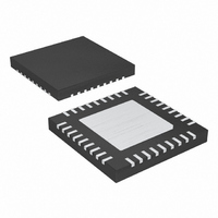
MAX8798ETX+ Maxim Integrated Products, MAX8798ETX+ Datasheet - Page 5

MAX8798ETX+
Manufacturer Part Number
MAX8798ETX+
Description
IC INTERNAL-SW BOOST REG 36-TQFN
Manufacturer
Maxim Integrated Products
Datasheet
1.MAX8798ETX.pdf
(31 pages)
Specifications of MAX8798ETX+
Applications
LCD Monitor, Notebook Display
Current - Supply
400µA
Voltage - Supply
1.8 V ~ 6 V
Operating Temperature
-40°C ~ 85°C
Mounting Type
Surface Mount
Package / Case
36-TQFN Exposed Pad
Operating Supply Voltage
1.8 V to 5.5 V
Maximum Operating Temperature
- 40 C
Mounting Style
SMD/SMT
Maximum Power Dissipation
2179.8 mW
Minimum Operating Temperature
+ 85 C
Supply Current
4 uA
Input Voltage
4V
Output Current
400mA
Output Voltage
18V
No. Of Outputs
2
Power Dissipation Pd
2.18W
Supply Voltage Range
1.8V To 5.5V
No. Of Pins
36
Operating Temperature Range
-40°C To +85°C
Rohs Compliant
Yes
Lead Free Status / RoHS Status
Lead free / RoHS Compliant
ELECTRICAL CHARACTERISTICS (continued)
(V
V
ELECTRICAL CHARACTERISTICS
(V
V
Output Slew Rate CKV, CKVB
Propagation Delay Between
STV and STVP
STVP Output Slew Rate
Charge-Sharing Discharge
Path Resistance
DISH Turn-On Threshold
STV, CPV, OE Input Low Voltage
STV, CPV, OE Input High Voltage
OECON Input Low Voltage
OECON Input High Voltage
OECON Sink Current
STV, CPV, OE
Input Current
CKV, CKVB, STVP Output
High-Impedance Current
CONTROL INPUTS
Input Low Voltage
Input High Voltage
V
V
V
IN Input Voltage Range
IN Quiescent Current
IN Undervoltage Lockout
STV
STV
IN
IN
Integrated 3-Channel Scan Driver for TFT LCDs
DD
DD
DD
= V
= V
= V
= V
Input Voltage Range
Quiescent Current
Undervoltage Lockout
Input Current
DD
DD
OECON
OECON
PARAMETER
= V
= V
PARAMETER
SHDN
SHDN
= 0, T
= 0, T
_______________________________________________________________________________________
= +3V, circuit of Figure 2, V
= +3V, circuit of Figure 2, V
A
A
= 0°C to +85°C, unless otherwise noted. Typical values are at T
= -40°C to +85°C, unless otherwise noted.) (Note 6)
Internal-Switch Boost Regulator with
Without charge sharing,
STV = V
C
C
CKV to CKVCS and
CKVB to CKVBCS
Dish falling
V
V
V
V
V
V
V
V
V
V
V
OECON
STV
CPV
OE
OECON
CKV
CKVB
CKVCS
CKVBCS
STVP
LOAD
LOAD
V
V
(Note 1)
V
V
= V
DD
DD
IN
IN
= V
= V
= GON or GOFF, high impedance
, 1.8V < V
, 3.0V < V
= GON or GOFF, high impedance
= GON or GOFF, high impedance
= 0 or 3V
= 4.7nF
= 4.7nF, 50
rising; typical hysteresis 100mV
= 3V, V
DD
= 3V
rising; typical hysteresis 100mV
DD
= GON or GOFF, high impedance
= 5V = V
DD
= V
DD
= GON or GOFF, high impedance
, C
or GND,
or GND,
DD
or GND,
BOOST
LOAD
BOOST
FB
or GND
IN
IN
= 1.5V, not switching
DD
< 3.0V
< 5.5V
= 4.7nF, 50
= 8V, V
= 8V, V
CONDITIONS
CONDITIONS
GON
GON
= 23V, V
= 23V, V
GOFF
GOFF
= -12V, V
= -12V, V
A
= +25°C.)
POS
POS
MIN
MIN
1.6
2.0
0.4
1.8
2.0
1.8
1.8
20
20
-1
-1
-1
= 0, V
= 0, V
NEG
NEG
TYP
TYP
250
250
0.8
40
40
= 1.5V, V
= 1.5V, V
MAX
MAX
450
400
1.75
1.75
-1.8
0.8
1.5
0.6
+1
+1
+1
4.0
6.0
0.1
10
OE
OE
= V
= V
UNITS
UNITS
V/μs
V/μs
mA
mA
CPV
μA
μA
μA
ns
μA
CPV
V
V
V
V
V
V
V
V
V
V
V
=
5
=


