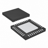
MAX8798ETX+ Maxim Integrated Products, MAX8798ETX+ Datasheet - Page 22

MAX8798ETX+
Manufacturer Part Number
MAX8798ETX+
Description
IC INTERNAL-SW BOOST REG 36-TQFN
Manufacturer
Maxim Integrated Products
Datasheet
1.MAX8798ETX.pdf
(31 pages)
Specifications of MAX8798ETX+
Applications
LCD Monitor, Notebook Display
Current - Supply
400µA
Voltage - Supply
1.8 V ~ 6 V
Operating Temperature
-40°C ~ 85°C
Mounting Type
Surface Mount
Package / Case
36-TQFN Exposed Pad
Operating Supply Voltage
1.8 V to 5.5 V
Maximum Operating Temperature
- 40 C
Mounting Style
SMD/SMT
Maximum Power Dissipation
2179.8 mW
Minimum Operating Temperature
+ 85 C
Supply Current
4 uA
Input Voltage
4V
Output Current
400mA
Output Voltage
18V
No. Of Outputs
2
Power Dissipation Pd
2.18W
Supply Voltage Range
1.8V To 5.5V
No. Of Pins
36
Operating Temperature Range
-40°C To +85°C
Rohs Compliant
Yes
Lead Free Status / RoHS Status
Lead free / RoHS Compliant
Internal-Switch Boost Regulator with
Integrated 3-Channel Scan Driver for TFT LCDs
The minimum inductance value, peak current rating, and
series resistance are factors to consider when selecting
the inductor. These factors influence the converter’s effi-
ciency, maximum output-load capability, transient
response time, and output-voltage ripple. Physical size
and cost are also important factors to be considered.
The maximum output current, input voltage, output volt-
age, and switching frequency determine the inductor
value. Very high inductance values minimize the cur-
rent ripple, and therefore, reduce the peak current that
decreases core losses in the inductor and I
the entire power path. However, large inductor values
also require more energy storage and more turns of
wire that increase physical size and can increase I
losses in the inductor. Low inductance values decrease
the physical size, but increase the current ripple and
peak current. Finding the best inductor involves choos-
ing the best compromise between circuit efficiency,
inductor size, and cost.
The equations used here include a constant called LIR
that is the ratio of the inductor peak-to-peak ripple cur-
rent to the average DC inductor current at the full-load
current. The best trade-off between inductor size and
circuit efficiency for step-up regulators generally has an
LIR between 0.3 and 0.5. However, depending on the
AC characteristics of the inductor core material and
ratio of inductor resistance to other power-path resis-
tances, the best LIR can shift up or down. If the induc-
tor resistance is relatively high, more ripple can be
accepted to reduce the number of turns required and
increase the wire diameter. If the inductor resistance is
relatively low, increasing inductance to lower the peak
current can decrease losses throughout the power
path. If extremely thin high-resistance inductors are
used, as is common for LCD panel applications, the
best LIR can increase to between 0.5 and 1.0.
Once a physical inductor is chosen, higher and lower
values of the inductor should be evaluated for efficien-
cy improvements in typical operating regions.
In Figure 2, the LCD’s gate-on and gate-off supply volt-
ages are generated from two unregulated charge
pumps driven by the step-up regulator’s LX node. The
additional load on LX must therefore be considered in
the inductance and current calculations. The effective
maximum output current, I
of the maximum load current of the step-up regulator’s
output plus the contributions from the positive and neg-
ative charge pumps:
22
______________________________________________________________________________________
Main Step-Up Regulator
MAIN(EFF)
Design Procedure
Inductor Selection
becomes the sum
2
R losses in
2
R
where I
rent, n
stages, n
stages, I
rent, and I
rent, assuming the initial pump source for I
V
Calculate the approximate inductor value using the typ-
ical input voltage (V
(I
an appropriate curve in the Typical Operating Char-
acteristics , and an estimate of LIR based on the above
discussion:
Choose an available inductor value from an appropriate
inductor family. Calculate the maximum DC input cur-
rent at the minimum input voltage V
servation of energy and the expected efficiency at that
operating point ( η
in the Typical Operating Characteristics :
Calculate the ripple current at that operating point and
the peak current required for the inductor:
The inductor’s saturation current rating and the
MAX8798’s LX current limit (I
and the inductor’s DC current rating should exceed
I
with less than 0.1Ω series resistance.
Considering Figure 2, the maximum load current
(I
input voltage of 3.3V. The effective full-load step-up
current is:
IN(DC,MAX)
MAIN
MAIN(EFF)
MAIN(MAX)
I
MAIN EFF
I
MAIN EFF
.
(
NEG
(
MAIN(MAX)
L
NEG
I
=
POS
RIPPLE
POS
)
)
), the expected efficiency ( η
⎛
⎜
⎝
. For good efficiency, choose an inductor
) is 300mA, with an 8V output and a typical
I
=
=
IN DCMAX
is the number of negative charge-pump
V
I
MAIN MAX
MAIN
I
300
is the negative charge-pump output cur-
(
V
PEAK
is the number of positive charge-pump
IN
is the positive charge-pump output cur-
=
mA
,
MIN
(
is the maximum step-up output cur-
⎞
⎟
⎠
V
=
2
IN MIN
+ ×
IN
⎛
⎜
⎝
I
) taken from an appropriate curve
)
IN DCMAX
(
2 20
I
)
MAIN EFF
=
), the maximum output current
(
+
L V
I
V
MAIN EFF
n
)
×
MAIN
V
NEG
,
×
mA
IN MIN
(
(
MAIN
(
V
LIM
(
MAIN
×
+
)
)
−
I
(
+
) should exceed I
NEG
×
2 1 20
V
)
)
×
I
IN
f
× η
RIPPLE
+ ×
OSC
×
f
−
OSC
V
)
IN(MIN)
2
+
V
MIN
MAIN
IN MIN
(
n
⎞
⎟
⎠
TYP
(
POS
⎛
⎜
⎝
mA
η
LIR
) taken from
TYP
)
+ ×
using con-
)
=
1
400
)
⎞
⎟
⎠
POS
I
POS
mA
PEAK
is


