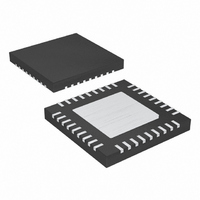
MAX8798ETX+ Maxim Integrated Products, MAX8798ETX+ Datasheet - Page 13

MAX8798ETX+
Manufacturer Part Number
MAX8798ETX+
Description
IC INTERNAL-SW BOOST REG 36-TQFN
Manufacturer
Maxim Integrated Products
Datasheet
1.MAX8798ETX.pdf
(31 pages)
Specifications of MAX8798ETX+
Applications
LCD Monitor, Notebook Display
Current - Supply
400µA
Voltage - Supply
1.8 V ~ 6 V
Operating Temperature
-40°C ~ 85°C
Mounting Type
Surface Mount
Package / Case
36-TQFN Exposed Pad
Operating Supply Voltage
1.8 V to 5.5 V
Maximum Operating Temperature
- 40 C
Mounting Style
SMD/SMT
Maximum Power Dissipation
2179.8 mW
Minimum Operating Temperature
+ 85 C
Supply Current
4 uA
Input Voltage
4V
Output Current
400mA
Output Voltage
18V
No. Of Outputs
2
Power Dissipation Pd
2.18W
Supply Voltage Range
1.8V To 5.5V
No. Of Pins
36
Operating Temperature Range
-40°C To +85°C
Rohs Compliant
Yes
Lead Free Status / RoHS Status
Lead free / RoHS Compliant
Integrated 3-Channel Scan Driver for TFT LCDs
PIN
10
11
12
13
14
15
16
17
18
19
1
2
3
4
5
6
7
8
9
CKVBCS
OECON
CKVCS
NAME
CKVB
SCLS
STVP
DISH
GND
WPN
CKV
WPP
CPV
SCL
SDA
STV
V
SET
OE
VL
DD
______________________________________________________________________________________
High-Voltage, Gate-Pulse Output. When enabled, CKV toggles between its high state (connected to
GON) and its low state (connected to GOFF) on each falling edge of the CPV input. Further, CKV is high
impedance whenever CPV and OE are both low or whenever CPV is low and OECON is high.
CKV Charge-Sharing Connection. CKVCS connects to CKV whenever CKV is high impedance to allow
connection to CKVB, sharing charge between the capacitive loads on these two outputs.
CKVB Charge-Sharing Connection. CKVBCS connects to CKVB whenever CKVB is high impedance to
allow connection to CKV, sharing charge between the capacitive loads on these two outputs.
High-Voltage, Gate-Pulse Output. CKVB is the inverse of CKV during active states and is high
impedance whenever CKV is high impedance.
High-Voltage, Start-Pulse Output. STVP is low (connected to GOFF) whenever STV is low and is high
(connected to GON) only when STV is high and CPV and OE are both low. When STV is high and either
CPV or OE is high, STVP is high impedance.
Vertical Sync Input. The rising edge of STV begins a frame of data. The STV input is used to generate the
high-voltage STVP output.
Active-Low, Output-Enable Timing Input. OECON is driven by an RC-filtered version of the OE input signal. If
OE remains high long enough for the resistor to charge the capacitor up to the OECON threshold, the OE
signal is masked until OE goes low and the capacitor is discharged below the threshold through the resistor.
Active-High, Gate-Pulse Output Enable. CKV and CKVB leave the high-impedance charge-sharing state
on the rising edge of OE.
Vertical Clock-Pulse Input. CPV controls the timing of the CKV and CKVB outputs that change state (by
first sharing charge) on its falling edge.
Logic Ground
GOFF Discharge Input. Pulling DISH below ground activates an internal connection between GOFF and
GND, rapidly discharging the GOFF supply. Typically, DISH is capacitively connected to IN, so that
when V
Supply Input. Logic supply input for the VCOM calibrator. Bypass to GND through a minimum 0.1μF
capacitor.
Active-Low, Write-Protect Input. When WPN is low, I
settings cannot be modified.
Alternate I
alternate clock source.
I
I
Write-Protect Output. WPP is the inverse of WPN. It can be used to control active-high, write-protect
inputs on other devices.
Full-Scale, Sink-Current Adjustment Input. Connect a resistor, R
scale adjustable sink current that is V
3.3V On-Chip Regulator Output. This regulator powers internal analog circuitry for the step-up regulator,
op amp, and VCOM calibrator. External loads up to 10mA can be powered. Bypass VL to GND with a
0.22μF or greater ceramic capacitor.
2
2
C-Compatible Clock Input and Output
C-Compatible Serial Bidirectional Data Line
Internal-Switch Boost Regulator with
IN
falls GOFF is discharged.
2
C-Compatible Clock Input. When WPN is high, SCLS connects to SCL to drive SCL from an
BOOST
/ (20 x R
FUNCTION
2
C commands are ignored and the VCOM calibrator
SET
). I
OUT
SET
is equal to the current through R
, from SET to GND to set the full-
Pin Description
SET
.
13


