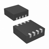
STM6510WCACDG6F STMicroelectronics, STM6510WCACDG6F Datasheet - Page 9

STM6510WCACDG6F
Manufacturer Part Number
STM6510WCACDG6F
Description
IC SMART RESET DUAL PB 8TDFN
Manufacturer
STMicroelectronics
Series
Smart Reset™r
Type
Smart Resetr
Specifications of STM6510WCACDG6F
Number Of Voltages Monitored
1
Output
Open Drain or Open Collector
Reset
Active Low
Reset Timeout
Adjustable/Selectable
Voltage - Threshold
1.665V
Operating Temperature
-40°C ~ 85°C
Mounting Type
Surface Mount
Package / Case
8-TDFN
Current - Supply
1.5µA
Voltage - Supply
1 V ~ 5.5 V
Applications
General Purpose
Supply Voltage (max)
7 V
Supply Voltage (min)
- 0.3 V
Maximum Operating Temperature
+ 85 C
Minimum Operating Temperature
- 40 C
Mounting Style
SMD/SMT
Number Of Switches
Dual
Supply Current
1.4 uA
Operating Temperature (max)
85C
Operating Temperature (min)
-40C
Pin Count
8
Mounting
Surface Mount
Case Length
2mm
Case Height
0.73mm
Screening Level
Industrial
Lead Free Status / RoHS Status
Lead free / RoHS Compliant
Other names
497-10536-2
Available stocks
Company
Part Number
Manufacturer
Quantity
Price
STM6510
1.3
1.3.1
1.3.2
1.3.3
1.3.4
Pin descriptions
Power supply (V
This pin is used to provide the power to the Smart Reset™ device and to monitor the power
supply. A 0.1 µF decoupling ceramic capacitor is recommended to be connected between
the V
Ground (V
This is the supply ground for the device.
Smart Reset™ push-button inputs (SR0, SR1)
Both SR0 and SR1 need to be held active at the same time for at least t
reset output pulse. Include an internal 65 kΩ pull-up resistor to V
Figure 6.
Adjustable delay of Smart Reset™ input (SRC pin)
This pin controls the setup time before the push-button action is validated by the reset
output. It is connected to an external capacitor (C
desired value of setup time (t
Calculated t
Table 2.
1. Example calculations based on an ideal capacitor. During application design and component selection it
2. In case of repeated activations of the t
Calculated C
should be considered that the current flowing into the external t
the order of 100 nA, therefore a low-leakage capacitor (ceramic or film capacitor) and an adequate PCB
environment should be used to prevent t
value of C
activations to fully discharge C
SR0
SR1
RST
value [µF]
CC
0.2
0.3
0.6
and V
1
SRC
SRC
Timing waveforms
t
SS
SRC
SRC
SS
is 0.01 µF.
)
and C
pins.
programmed by an ideal external capacitor
CC
SRC
)
Min.
10
examples are given in
2
3
6
SRC
SRC
Doc ID 16788 Rev 2
, so that the next t
).
SRC
Setup delay t
SRC
counter, an interval of 10 ms min. is needed between the
accuracy from being affected. A recommended minimum
Typ.
4.5
15
SRC
3
9
t SRC
SRC
is as specified.
SRC
Table
[s]
), which is tied to ground to provide the
(1)(2)
SRC
2. Refer also to
programming capacitor (C
t REC
Max.
12
20
4
6
CC
for each input.
Table
SRC
Closest common
C
to activate the
SRC
6.
SRC
Description
value [µF]
0.22
0.33
0.56
) is on
1
AM00393
9/26


