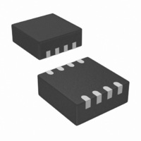
STM6510WCACDG6F STMicroelectronics, STM6510WCACDG6F Datasheet - Page 15

STM6510WCACDG6F
Manufacturer Part Number
STM6510WCACDG6F
Description
IC SMART RESET DUAL PB 8TDFN
Manufacturer
STMicroelectronics
Series
Smart Reset™r
Type
Smart Resetr
Specifications of STM6510WCACDG6F
Number Of Voltages Monitored
1
Output
Open Drain or Open Collector
Reset
Active Low
Reset Timeout
Adjustable/Selectable
Voltage - Threshold
1.665V
Operating Temperature
-40°C ~ 85°C
Mounting Type
Surface Mount
Package / Case
8-TDFN
Current - Supply
1.5µA
Voltage - Supply
1 V ~ 5.5 V
Applications
General Purpose
Supply Voltage (max)
7 V
Supply Voltage (min)
- 0.3 V
Maximum Operating Temperature
+ 85 C
Minimum Operating Temperature
- 40 C
Mounting Style
SMD/SMT
Number Of Switches
Dual
Supply Current
1.4 uA
Operating Temperature (max)
85C
Operating Temperature (min)
-40C
Pin Count
8
Mounting
Surface Mount
Case Length
2mm
Case Height
0.73mm
Screening Level
Industrial
Lead Free Status / RoHS Status
Lead free / RoHS Compliant
Other names
497-10536-2
Available stocks
Company
Part Number
Manufacturer
Quantity
Price
STM6510
Table 6.
1. Valid for ambient operating temperature: T
2. Typical value is at 25 °C and V
3. For devices with V
4. Guaranteed by design.
5. Input glitch immunity is equal to t
Symbol
Smart Reset™ inputs
t
t
V
REC
SRC
V
R
V
V
HYST
V
I
V
CC
RST
PUI
CC
OL
IH
IL
(4)
(5)
Supply voltage range
Supply current (V
Reset output voltage low
V
threshold (refer to
Hysteresis of V
V
User-adjustable reset timeout
period on RST. Refer to
Table
User-adjustable delayed Smart
Reset™ setup time. Refer to
Table
SR0, SR1 input voltage low
SR0, SR1 input voltage high
Internal pull-up resistor, SR0,
SR1 inputs
CC
CC
DC and AC characteristics
undervoltage reset
to reset delay
3.
2.
RST
Parameter
< 3.0 V.
RST
CC
(4)
Table
)
CC
SRC
= 3.3 V unless otherwise noted.
7)
(when both SR inputs are low, otherwise infinite).
A
= –40 to +85 °C; V
V
V
V
V
V
–40 to +85 °C
25 °C
L, M
T, S, R, Z, Y, W, V
V
to (V
Reset output valid - active-low
CC
CC
CC
CC
CC
CC
Doc ID 16788 Rev 2
falling from (V
= 5.0 V
= 3.0 V
RST
≥ 4.5 V, sinking 3.2 mA
≥ 3.3 V, sinking 2.5 mA
≥ 1.0 V, sinking 0.1 mA
Test conditions
- 100 mV) at 10 mV/µs
(3)
CC
RST
= 1.0 to 5.5 V (except where noted).
+ 100 mV)
(1)
10 000 x
0.7 V
–2.5%
–2.0%
C
C
V
V
Min.
10 x
(µF)
(µF)
1.0
tREC
RST
RST
SRC
CC
DC and AC parameters
15 000 x
Typ.
C
C
V
V
0.5%
(µF)
15 x
(µF)
1%
1.5
1.4
tREC
20
65
SRC
RST
RST
(2)
20 000 x
0.3 V
+2.5%
+2.0%
C
C
Max.
V
V
20 x
(µF)
(µF)
5.5
2.4
0.3
0.3
0.3
tREC
RST
RST
SRC
CC
Units
15/26
ms
kΩ
µA
µA
µs
V
V
V
V
V
V
V
V
s


