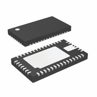
LTC3577EUFF#PBF Linear Technology, LTC3577EUFF#PBF Datasheet - Page 30

LTC3577EUFF#PBF
Manufacturer Part Number
LTC3577EUFF#PBF
Description
IC PWR MANAGEMENT HANDHELD 44QFN
Manufacturer
Linear Technology
Datasheet
1.LTC3577EUFFPBF.pdf
(54 pages)
Specifications of LTC3577EUFF#PBF
Applications
Handheld/Mobile Devices
Voltage - Supply
4.35 V ~ 5.5 V
Operating Temperature
-40°C ~ 85°C
Mounting Type
Surface Mount
Package / Case
44-QFN
Lead Free Status / RoHS Status
Lead free / RoHS Compliant
Current - Supply
-
Available stocks
Company
Part Number
Manufacturer
Quantity
Price
OPERATION
LTC3577/LTC3577-1
Each input is protected up to the drain-source breakdown,
BVDSS, of MN1 and MN2. R1 must also be rated for the
power dissipated during maximum overvoltage. See the
“Overvoltage Protection” section for an explanation of
this calculation. Table 2 shows some NMOS FETs that are
suitable for overvoltage protection.
Table 2. Recommended Overvoltage FETs
Reverse Input Voltage Protection
The LTC3577 can also be easily protected against the
application of reverse voltage as shown in Figure 10. D1
and R1 are necessary to limit the maximum VGS seen by
MP1 during positive overvoltage events. D1’s breakdown
voltage must be safely below MP1’s BVGS. The circuit
shown in Figure 11 offers forward voltage protection up
to MN1’s BVDSS and reverse voltage protection up to
MP1’s BVDSS.
LOW DROPOUT LINEAR REGULATOR OPERATION
LDO Operation and Voltage Programming
The LTC3577 contains two 150mA adjustable output LDO
regulators. To enable the LDOs write a 1 to the LDO1EN
and/or LDO2EN I
three ways: 1) Write a 0 to the LDO1EN and LDO2EN
registers; 2) Bring DV
threshold; 3) Enter the power-down pushbutton state.
30
IRLML2502
Si2302ADS
Si2306BDS
Si2316BDS
NMOS FET
Si1472DH
V1
V2
Figure 10. Dual Input Overvoltage Protection
D2
2
C registers. The LDOs can be disabled
BVDSS
30V
20V
30V
30V
20V
R1
D1
CC
MN1
MN2
below the DV
C1
82mΩ
60mΩ
65mΩ
80mΩ
35mΩ
R
ON
WALL
OVGATE
V
OVSENS
BUS
LTC3577
CC
undervoltage
3577 F10
PACKAGE
SC70-6
SOT-23
SOT-23
SOT-23
SOT-23
The LDOs are further disabled if V
UVLO threshold and cannot be enabled until the UVLO
condition is removed.
When disabled all LDO circuitry is powered off leaving only
a few nanoamps of leakage current on the LDO supply.
The LDO outputs are individually pulled to ground through
internal resistors when disabled.
The power good status bits of LDO1 and LDO2 are avail-
able in I
PGLDO[2] for LDO1 and LDO2 respectively. The power
good comparators for both LDOs are sampled when the
I
Figure 12 shows the LDO application circuit. The full-
scale output voltage for each LDO is programmed using
a resistor divider from the LDO output (LDO1 or LDO2)
connected to the feedback pins (LDO1_FB or LDO2_FB)
such that:
2
C port receives the correct I
V
USB/WALL
LDOx
ADAPTER
LDOxEN
2
C through the read-back registers PGLDO[1] and
Figure 11. Dual Polarity Voltage Protection
= 0.8V •
0
1
Figure 12. LDO Application Circuit
MP1
D1: 5.6V ZENER
MP1: Si2323DS, BVDSS = 20V
V
V
BUS
BUS
GND
R1
500k
⎛
⎝ ⎜
POSITIVE PROTECTION UP TO BVDSS OF MN1
NEGATIVE PROTECTION UP TO BVDSS OF MP1
R2
R1
V
INLDOx
D1
+ 1
MP
⎞
⎠ ⎟
LDOx_FB
0.8V
R2
6.2k
MN1
LDOx
2
C read address.
OUT
R1
R2
3577 F12
C1
falls below the V
V
OVGATE
OVSENS
BUS
LTC3577
C
OUT
LDOx
OUTPUT
3577 F11
3577fa
OUT


