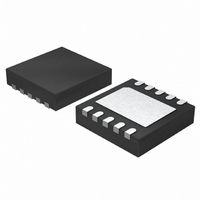
LTC3588EDD-1#PBF Linear Technology, LTC3588EDD-1#PBF Datasheet - Page 8

LTC3588EDD-1#PBF
Manufacturer Part Number
LTC3588EDD-1#PBF
Description
IC ENEGRY HARVESTING PSU 10DFN
Manufacturer
Linear Technology
Datasheet
1.LTC3588EDD-1PBF.pdf
(20 pages)
Specifications of LTC3588EDD-1#PBF
Applications
Energy Harvesting
Voltage - Supply
2.7 V ~ 20 V
Operating Temperature
-40°C ~ 85°C
Mounting Type
Surface Mount
Package / Case
10-DFN
Ic Function
Power Management IC
Supply Voltage Range
2.7V To 20V
Operating Temperature Range
-40°C To +85°C
Digital Ic Case Style
DFN
No. Of Pins
10
Msl
MSL 1 - Unlimited
Rohs Compliant
Yes
Lead Free Status / RoHS Status
Lead free / RoHS Compliant
Current - Supply
-
Available stocks
Company
Part Number
Manufacturer
Quantity
Price
LTC3588-1
OPERATION
The LTC3588-1 is an ultralow quiescent current power
supply designed specifi cally for energy harvesting and/or
low current step-down applications. The part is designed to
interface directly to a piezoelectric or alternative A/C power
source, rectify a voltage waveform and store harvested
energy on an external capacitor, bleed off any excess power
via an internal shunt regulator, and maintain a regulated
output voltage by means of a nanopower high effi ciency
synchronous buck regulator.
Internal Bridge Rectifi er
The LTC3588-1 has an internal full-wave bridge rectifi er
accessible via the differential PZ1 and PZ2 inputs that
rectifi es AC inputs such as those from a piezoelectric
element. The rectifi ed output is stored on a capacitor at
the V
buck converter. The low-loss bridge rectifi er has a total
drop of about 400mV with typical piezo generated currents
(~10μA). The bridge is capable of carrying up to 50mA.
One side of the bridge can be operated as a single-ended
DC input. PZ1 and PZ2 should never be shorted together
when the bridge is in use.
Undervoltage Lockout (UVLO)
When the voltage on V
threshold the buck converter is enabled and charge is
transferred from the input capacitor to the output capacitor.
A wide (~1V) UVLO hysteresis window is employed
with a lower threshold approximately 300mV above the
selected regulated output voltage to prevent short cycling
during buck power-up. When the input capacitor voltage
is depleted below the UVLO falling threshold the buck
converter is disabled. Extremely low quiescent current
(450nA typical) in UVLO allows energy to accumulate on
the input capacitor in situations where energy must be
harvested from low power sources.
8
IN
pin and can be used as an energy reservoir for the
IN
rises above the UVLO rising
Buck Operation
The buck regulator uses a hysteretic voltage algorithm
to control the output through internal feedback from the
V
capacitor through an inductor to a value slightly higher than
the regulation point. It does this by ramping the inductor
current up to 260mA through an internal PMOS switch
and then ramping it down to 0mA through an internal
NMOS switch. This effi ciently delivers energy to the output
capacitor. The ramp rate is determined by V
the inductor value. If the input voltage falls below the
Internal Rail Generation
Two internal rails, CAP and V
are used to drive the high side PMOS and low side NMOS
of the buck converter, respectively. Additionally the V
rail serves as logic high for output voltage select bits D0
and D1. The V
the CAP rail is regulated at 4.8V below V
intended to be used as external rails. Bypass capacitors
are connected to the CAP and V
reservoirs for driving the buck switches. When V
4.8V, V
shows the ideal V
OUT
sense pin. The buck converter charges an output
IN2
Figure 1. Ideal V
is equal to V
18
16
14
12
10
8
6
4
2
0
IN2
0
rail is regulated at 4.8V above GND while
IN
, V
IN
IN2
IN
5
, V
and CAP is held at GND. Figure 1
and CAP relationship.
IN2
V
IN2
IN
CAP
(V)
and CAP Relationship
, are generated from V
V
IN2
IN
10
pins to serve as energy
V
IN2
IN
35881 F01
. These are not
15
IN
, V
IN
OUT
is below
IN
, and
35881fa
and
IN2


