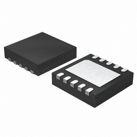
LTC3588EDD-1#PBF Linear Technology, LTC3588EDD-1#PBF Datasheet - Page 4

LTC3588EDD-1#PBF
Manufacturer Part Number
LTC3588EDD-1#PBF
Description
IC ENEGRY HARVESTING PSU 10DFN
Manufacturer
Linear Technology
Datasheet
1.LTC3588EDD-1PBF.pdf
(20 pages)
Specifications of LTC3588EDD-1#PBF
Applications
Energy Harvesting
Voltage - Supply
2.7 V ~ 20 V
Operating Temperature
-40°C ~ 85°C
Mounting Type
Surface Mount
Package / Case
10-DFN
Ic Function
Power Management IC
Supply Voltage Range
2.7V To 20V
Operating Temperature Range
-40°C To +85°C
Digital Ic Case Style
DFN
No. Of Pins
10
Msl
MSL 1 - Unlimited
Rohs Compliant
Yes
Lead Free Status / RoHS Status
Lead free / RoHS Compliant
Current - Supply
-
Available stocks
Company
Part Number
Manufacturer
Quantity
Price
LTC3588-1
ELECTRICAL CHARACTERISTICS
Note 1: Stresses beyond those listed under Absolute Maximum Ratings
may cause permanent damage to the device. Exposure to any Absolute
Maximum Rating condition for extended periods may affect device
reliability and lifetime.
Note 2: The LTC3588-1 is tested under pulsed load conditions such
that T
from 0°C to 85°C junction temperature. Specifi cations over the –40°C
to 125°C operating junction temperature range are assured by design,
characterization, and correlation with statistical process controls.
The LTC3588I-1 is guaranteed over the full –40°C to 125°C operating
TYPICAL PERFORMANCE CHARACTERISTICS
4
1000
900
800
700
600
500
400
300
200
100
4.2
4.0
3.8
3.6
3.4
3.2
3.0
2.8
J
0
≈ T
–55
0
I
UVLO Falling vs Temperature
VIN
D1 = D0 = 1
A
. The LTC3588E-1 is guaranteed to meet specifi cations
–35
in UVLO vs V
1
–15
TEMPERATURE (°C)
5
2
25
V
IN
D1 = D0 = 1
D1 = 1, D0 = 0
D1 = D0 = 0
3
IN
(V)
45
–40°C
65
85°C
25°C
4
85
5
105
35881 G04
35881 G01
125
6
2400
2200
2000
1800
1600
1400
1200
1000
21.0
20.8
20.6
20.4
20.2
20.0
19.8
19.6
19.4
19.2
19.0
800
600
400
–55
2
I
V
VIN
D1 = D0 = 0
SHUNT
–35
4
in Sleep vs V
–15
vs Temperature
6
TEMPERATURE (°C)
5
I
8
SHUNT
25
V
I
IN
SHUNT
10
junction temperature range. Note that the maximum ambient temperature
consistent with these specifi cations is determined by specifi c operating
conditions in conjunction with board layout, the rated package thermal
impedance and other environmental factors.
Note 3: The junction temperature (T
temperature (T
to the formula: T
thermal impedance.
Note 4: Dynamic supply current is higher due to gate charge being
delivered at the switching frequency.
IN
(V)
= 25mA
45
12
= 1mA
–40°C
65
85°C
25°C
14
85 105
16
A
35881 G02
35881 G05
, in °C) and power dissipation (P
J
= T
125
18
A
+ (P
D
1800
1600
1400
1200
1000
• θ
800
600
400
200
5.2
5.0
4.8
4.6
4.4
4.2
4.0
3.8
0
JA
–55
1μ
UVLO Rising vs Temperature
Total Bridge Rectifi er Drop
vs Bridge Current
), where θ
|V
J
PZ1
–35
, in °C) is calculated from the ambient
– V
10μ
–15
PZ2
JA
BRIDGE CURRENT (A)
| – V
TEMPERATURE (°C)
5
(in °C/W) is the package
D
IN
100μ
, in Watts) according
25
D1 = D0 = 1
D1 = D0 = 0
45
–40°C
1m
65
85
25°C
10m
85°C
105
35881 G03
35881 G06
35881fa
125


