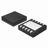
LTC3588EDD-1#PBF Linear Technology, LTC3588EDD-1#PBF Datasheet - Page 12

LTC3588EDD-1#PBF
Manufacturer Part Number
LTC3588EDD-1#PBF
Description
IC ENEGRY HARVESTING PSU 10DFN
Manufacturer
Linear Technology
Datasheet
1.LTC3588EDD-1PBF.pdf
(20 pages)
Specifications of LTC3588EDD-1#PBF
Applications
Energy Harvesting
Voltage - Supply
2.7 V ~ 20 V
Operating Temperature
-40°C ~ 85°C
Mounting Type
Surface Mount
Package / Case
10-DFN
Ic Function
Power Management IC
Supply Voltage Range
2.7V To 20V
Operating Temperature Range
-40°C To +85°C
Digital Ic Case Style
DFN
No. Of Pins
10
Msl
MSL 1 - Unlimited
Rohs Compliant
Yes
Lead Free Status / RoHS Status
Lead free / RoHS Compliant
Current - Supply
-
Available stocks
Company
Part Number
Manufacturer
Quantity
Price
APPLICATIONS INFORMATION
LTC3588-1
PGOOD Signal
The PGOOD signal can be used to enable a sleeping
microprocessor or other circuitry when V
regulation, as shown in Figure 5. Typically V
somewhere between the UVLO thresholds at this time and
a load could only be supported by the output capacitor.
Alternatively, waiting a period of time after PGOOD goes
high would let the input capacitor accumulate more energy
allowing load current to be maintained longer as the buck
effi ciently transfers that energy to the output. While active,
a microprocessor may draw a small load when operating
sensors, and then draw a large load to transmit data.
Figure 5 shows the LTC3588-1 responding smoothly to
such a load step.
Input and Output Capacitor Selection
The input and output capacitors should be selected
based on the energy needs and load requirements of the
application. In every case the V
rated to withstand the highest voltage ever present at V
For 100mA or smaller loads, storing energy at the input
takes advantage of the high voltage input since the buck
can deliver 100mA average load current effi ciently to the
output. The input capacitor should then be sized to store
enough energy to provide output power for the length of
time required. This may involve using a large capacitor,
letting V
12
10μF
25V
IN
charge to a high voltage, or both. Enough energy
1μF
6V
4.7μF
6V
PZ1
V
CAP
V
D1
D0
IN
IN2
MIDE V21BL
LTC3588-1
GND
Figure 5. 3.3V Piezoelectric Energy Harvester Powering a Microprocessor
with a Wireless Transmitter and 50mA Load Step Response
PGOOD
V
PZ2
OUT
SW
IN
capacitor should be
10μH
3.3V
OUT
IN
47μF
6V
reaches
will be
EN
CORE
MICROPROCESSOR
35881 F05a
IN
GND
.
should be stored on the input so that the buck does not
reach the UVLO falling threshold which would halt energy
transfer to the output. In general:
The above equation can be used to size the input capaci-
tor to meet the power requirements of the output for the
desired duration. Here η is the average effi ciency of the
buck converter over the input range and V
voltage when the buck begins to switch. This equation
may overestimate the input capacitor necessary since load
current can deplete the output capacitor all the way to the
lower PGOOD threshold. It also assumes that the input
source charging has a negligible effect during this time.
The duration for which the regulator sleeps depends on
the load current and the size of the output capacitor. The
sleep time decreases as the load current increases and/or
as the output capacitor decreases. The DC sleep hysteresis
window is ±12mV around the programmed output volt-
age. Ideally this means that the sleep time is determined
by the following equation:
T
X
P
V
t
SLEEP
LOAD
UVLOFALLING
t
LOAD
AC-COUPLED
= C
25mA/DIV
20mV/DIV
CURRENT
VOLTAGE
OUTPUT
OUT
LOAD
=
5mA
≤ V
2
1
24mV
I
LOAD
ηC
V
L = 10μH, C
LOAD STEP BETWEEN 5mA and 55mA
IN
IN
= 5V
IN
≤ V
(
V
SHUNT
OUT
IN
2
= 47μF
− V
250μs/DIV
UVLOFALLING
IN
is the input
2
)
35881 F05b
35881fa


