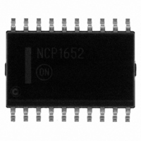
NCP1652DWR2G ON Semiconductor, NCP1652DWR2G Datasheet - Page 4

NCP1652DWR2G
Manufacturer Part Number
NCP1652DWR2G
Description
IC PFC CONTROLLER CCM/DCM 20SOIC
Manufacturer
ON Semiconductor
Datasheet
1.NCP1652DR2G.pdf
(34 pages)
Specifications of NCP1652DWR2G
Mode
Continuous Conduction (CCM), Discontinuous Conduction (DCM)
Frequency - Switching
100kHz
Current - Startup
5.62mA
Voltage - Supply
9.3 V ~ 20 V
Operating Temperature
-40°C ~ 125°C
Mounting Type
Surface Mount
Package / Case
20-SOIC (7.5mm Width)
Switching Frequency
20 KHz to 250 KHz
Maximum Operating Temperature
+ 125 C
Mounting Style
SMD/SMT
Minimum Operating Temperature
- 40 C
Lead Free Status / RoHS Status
Lead free / RoHS Compliant
Other names
NCP1652DWR2GOSTR
PIN FUNCTION DESCRIPTION
16 Pin
10
12
13
14
15
16
11
1
2
3
4
5
6
7
8
9
Pin
20 Pin
10
11
12
13
14
15
16
17
18
19
20
1
2
3
4
5
6
7
8
9
RAMP COMP
AC COMP
Symbol
Rdelay
OUTB
AC IN
OUTA
Latch
GND
I
VFF
I
V
Spos
CM
NC
NC
NC
NC
FB
AVG
HV
C
CC
T
An external timing capacitor (C
V sets the oscillator frequency and the gain of the multiplier.
A resistor (R
added to the current signal. Ramp compensation is required to prevent subharmonic oscilla-
tions. This pin should not be left open.
The scaled version of the full wave rectified input ac wave is connected to this pin by means of
a resistive voltage divider. The line voltage information is used by the multiplier.
An error signal from an external error amplifier circuit is fed to this pin via an optocoupler or
other isolation circuit. The FB voltage is a proportional of the load of the converter. If the voltage
on the FB pin drops below V
Feedforward input. A scaled version of the filtered rectified line voltage is applied by means of a
resistive divider and an averaging capacitor. The information is used by the Reference Generat-
or to regulate the controller.
Multiplier output. A capacitor is connected between this pin and ground to filter the modulated
output of the multiplier.
Sets the pole for the ac reference amplifier. The reference amplifier compares the low fre-
quency component of the input current to the ac reference signal. The response must be slow
enough to filter out most of the high frequency content of the current signal that is injected from
the current sense amplifier, but fast enough to cause minimal distortion to the line frequency
information. The pin should not be left open.
Latch−Off input. Pulling this pin below 1.0 V (typical) or pulling it above 7.0 V (typical) latches
the controller. This input can be used to implement an overvoltage detector, an overtemperature
detector or both. Refer to Figure 69 for a typical implementation.
A resistor between this pin and ground sets the non−overlap time delay between OUTA and
OUTB. The delay is adjusted to prevent cross conduction between the primary MOSFET and
synchronous rectification MOSFET or optimize the resonant transition in an active clamp stage.
An external resistor and capacitor connected from this terminal to ground, to set and stabilizes
the gain of the current sense amplifier output that drives the ac error amplifier.
Positive current sense input. Connects to the positive side of the current sense resistor.
Positive input supply. This pin connects to an external capacitor for energy storage. An internal
current source supplies current from the STARTUP pin V
approximately 15.3 V, the current source turns off and the outputs are enabled. The drivers are
disabled once V
tup current is reduced to less than 500 mA.
Drive output for the main flyback power MOSFET or IGBT. OUTA has a source resistance of
13 W (typical) and a sink resistance of 8 W (typical).
Secondary output of the PWM Controller. It can be used to drive synchronous rectifier, and
active clamp switch, or both. OUTB has source and sink resistances of 22 W (typical) and 11
(typical), respectively.
Ground reference for the circuit.
Connect the rectified input line voltage directly to this pin to enable the internal startup regulator.
A constant current source supplies current from this pin to the capacitor connected to the V
pin, eliminating the need for a startup resistor. The charge current is typically 5.5 mA. Maximum
input voltage is 500 V.
RC
) between this pin and ground adjust the amount of ramp compensation that is
CC
http://onsemi.com
reaches approximately 10.3 V. If V
4
SSKIP
T
) sets the oscillator frequency. A sawtooth between 0.2 V and 4
the controller enters Soft−Skip™ to reduce acoustic noise.
Description
CC
CC
drops below 0.85 V (typical), the star-
. Once the voltage on V
CC
reaches
CC


