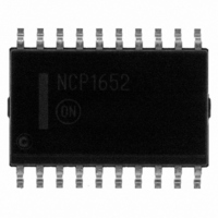
NCP1652DWR2G ON Semiconductor, NCP1652DWR2G Datasheet - Page 19

NCP1652DWR2G
Manufacturer Part Number
NCP1652DWR2G
Description
IC PFC CONTROLLER CCM/DCM 20SOIC
Manufacturer
ON Semiconductor
Datasheet
1.NCP1652DR2G.pdf
(34 pages)
Specifications of NCP1652DWR2G
Mode
Continuous Conduction (CCM), Discontinuous Conduction (DCM)
Frequency - Switching
100kHz
Current - Startup
5.62mA
Voltage - Supply
9.3 V ~ 20 V
Operating Temperature
-40°C ~ 125°C
Mounting Type
Surface Mount
Package / Case
20-SOIC (7.5mm Width)
Switching Frequency
20 KHz to 250 KHz
Maximum Operating Temperature
+ 125 C
Mounting Style
SMD/SMT
Minimum Operating Temperature
- 40 C
Lead Free Status / RoHS Status
Lead free / RoHS Compliant
Other names
NCP1652DWR2GOSTR
Introduction
PFC and an isolated step down ac−dc power conversion in
a single stage, resulting in a lower cost and reduced part
count solution. This controller is ideal for notebook
adapters, battery chargers and other off−line applications
with power requirements between 75 W and 150 W with an
output voltage greater than 12 V. The single stage is based
on the flyback converter and it is designed to operate in CCM
or DCM modes.
Power Factor Correction (PFC) Introduction
off−line power supplies to maximize the real power
available from the mains. Ideally, the electrical appliance
should present a load that emulates a pure resistor, in which
case the reactive power drawn by the device is zero. Inherent
in this scenario is the freedom from input current harmonics.
The current is a perfect replica of the input voltage (usually
a sine wave) and is exactly in phase with it. In this case the
current drawn from the mains is at a minimum for the real
power required to perform the needed work, and this
minimizes losses and costs associated not only with the
distribution of the power, but also with the generation of the
power and the capital equipment involved in the process.
The freedom from harmonics also minimizes interference
with other devices being powered from the same source.
supplies is to comply with regulatory requirements. Today,
electrical equipment in Europe must comply with the
European Norm EN61000−3−2. This requirement applies to
most electrical appliances with input power of 75 W or
greater, and it specifies the maximum amplitude of
line−frequency harmonics up to and including the 39
harmonic. While this requirement is not yet in place in the
US, power supply manufacturers attempting to sell products
worldwide are designing for compliance with this
requirement.
Typical Power Supply with PFC
preregulator creating an intermediate X400 V bus and an
isolated dc−dc converter producing the desired output
voltage as shown in Figure 51. This architecture has two
power stages.
individual power stage. It is commonly used because of
AC
Input
The NCP1652 is a highly integrated controller combining
Power factor correction shapes the input current of
Another reason to employ PFC in many of today’s power
A typical power supply consists of a boost PFC
A two stage architecture allows optimization of each
Figure 51. Typical Two Stage Power Converter
Rectifier
Filter
&
Preregulator
PFC
with isolator
DETAILED DEVICE DESCRIPTION
Converter
DC−DC
http://onsemi.com
V
out
th
19
designer familiarity and a vast range of available
components. But, because it processes the power twice, the
search is always on for a more compact and power efficient
solution.
shrinking the front−end converter (PFC preregulator) and
the dc−dc converter into a single power processing stage as
shown in Figure 52.
The NCP1652 based solution requires only one each of
MOSFET, magnetic element, output rectifier (low voltage)
and output capacitor (low voltage). In contrast, the 2−stage
solution requires two or more of the above−listed
components.
components (e.g. high voltage capacitor and high voltage
PFC diode) has significant impact on the system design. The
resultant cost savings and reliability improvement are often
worth the effort of designing a new converter.
Single PFC Stage
important to recognize that it is not a recommended solution
for all requirements. The following three limitations apply
to the single stage approach:
•
•
•
AC
Input
The NCP1652 controller offers the convenience of
This approach significantly reduces the component count.
While the single stage offers certain benefits, it is
The output voltage ripple will have a 2x line frequency
component (120 Hz for North American applications)
that can not be eliminated easily. The cause of this
ripple is the elimination of the energy storage element
that is typically the boost output capacitor in the
2−stage solution. The only way to reduce the ripple is to
increase the output filter capacitance. The required
value of capacitance is inversely proportional to the
output voltage – hence this approach is not
recommended for low voltage outputs such as 3.3 V or
5 V. However, if there is a follow−on dc−dc converter
stage or a battery after the single stage converter, the
low frequency ripple should not cause any concerns.
The hold−up time will not be as good as the 2−stage
approach – again due to the lack of an intermediate
energy storage element.
In a single stage converter, one FET processes all the
power – that is both a benefit and a limitation as the
stress on that main MOSFET is relatively higher.
Similarly, the magnetic component (flyback
transformer/inductor) can not be optimized as well as in
Figure 52. Single Stage Power Converter
Rectifier
Filter
&
Elimination
Flyback Converter
NCP1652 Based
of
Single−Stage
certain
high−voltage
V
out


