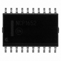
NCP1652DWR2G ON Semiconductor, NCP1652DWR2G Datasheet - Page 30

NCP1652DWR2G
Manufacturer Part Number
NCP1652DWR2G
Description
IC PFC CONTROLLER CCM/DCM 20SOIC
Manufacturer
ON Semiconductor
Datasheet
1.NCP1652DR2G.pdf
(34 pages)
Specifications of NCP1652DWR2G
Mode
Continuous Conduction (CCM), Discontinuous Conduction (DCM)
Frequency - Switching
100kHz
Current - Startup
5.62mA
Voltage - Supply
9.3 V ~ 20 V
Operating Temperature
-40°C ~ 125°C
Mounting Type
Surface Mount
Package / Case
20-SOIC (7.5mm Width)
Switching Frequency
20 KHz to 250 KHz
Maximum Operating Temperature
+ 125 C
Mounting Style
SMD/SMT
Minimum Operating Temperature
- 40 C
Lead Free Status / RoHS Status
Lead free / RoHS Compliant
Other names
NCP1652DWR2GOSTR
amplifier output is nearly saturated in a low state. While the
ac error amplifier output is saturated, I
not contribute to the voltage across the internal 21.33 kW
resistor on the PWM comparator non-inverting input. In this
operation mode, the voltage across the 21.33 kW resistor is
determined solely by the ramp compensation and the
instantaneous switch current as given by Equation 22.
V
provide some margin. The maximum instantaneous switch
current voltage contribution, V
Equation 23.
V
R
Replacing Equation 24 in Equation 21 we obtain:
PWM Logic
comparator, an RS flip-flop (latch) and an OR gate. The
REF(PWM)
REF(PWM)
RCOMP,
At low line and full load, the output of the ac error
The voltage reference of the PWM Comparator,
Substituting Equation 23 in Equation 22,
The PWM and logic circuits are comprised of a PWM
R
RCOMP
R
Equation 24 is obtained.
CS
R
V
V
, is 4 V. For these calculations, 3.8 V is used to
CS
ref(PWM)
at 3.8 V (provides margin) and solving for
+
RCOMP
+
+
V
N
N
P
S
N
N
INST
3.8 * 5.333 @ I
@
S
P
+
+ V
A
@
HF
dt
+ I
T @ A
primary
@V
di
L
RCOMP
102.38k
PK
out
P
HF
L
@t
3.8
@ R
P
on
@ T @ R
@ V
@ 102.38k
CS
@
PK
) 5.333 I
out
t
T
on
@ A
@ R
INST
ACEA
@ R
CS
HF
) V
CS
, is given by
@ A
RCOMP
is zero and does
@
INST
PK
HF
t
T
on
(eq. 20)
(eq. 21)
(eq. 22)
(eq. 23)
(eq. 24)
(eq. 25)
http://onsemi.com
setting
30
latch is Set dominant which means that if both R and S are
high the S signal will dominate and Q will be high, which
will hold the power switch off.
based on a fixed frequency oscillator. The oscillator
generates a voltage ramp as well as a pulse in sync with the
falling edge of the ramp. The pulse is an input to the PWM
Logic and Driver block. While the oscillator pulse is present,
the latch is reset, and the output drive is in its low state. On
the falling edge of the pulse, the OUTA goes high and the
power switch begins conduction.
current proportional to the ac error amplifier output voltage.
This complex waveform is compared to the 4 V reference
signal on the PWM comparator inverting input. When the
signal at the non-inverting input to the PWM comparator
exceeds 4 V, the output of the PWM comparator toggles to
a high state which drives the Set input of the latch and turns
the power switch off until the next clock cycle.
Brown−Out
to prevent the controller operate at low ac line voltages and
reduce stress in power components. A scaled version of the
rectified line voltage is applied to the VFF Pin by means of
a resistor divider. This voltage is used by the brown out
detector.
is below the brown−out exit threshold, V
0.45 V. The brown−out detector has 180 mV hysteresis. The
controller is enabled once V
reaches V
shows the relationship between the brown−out, V
and OUTB signals.
The NCP1652 uses a pulse width modulation scheme
The instantaneous inductor current is summed with a
The NCP1652 incorporates a brown−out detection circuit
A brown−out condition exists if the feedforward voltage
CC(on)
. OUTB is the last drive pulse. Figure 68
FF
is above 0.63 V and V
BO(high)
CC
, typically
, OUTA
CC


