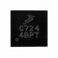
MPC17C724EP Freescale Semiconductor, MPC17C724EP Datasheet - Page 9

MPC17C724EP
Manufacturer Part Number
MPC17C724EP
Description
IC MOTOR DRVR H-BRDG DUAL 16-QFN
Manufacturer
Freescale Semiconductor
Type
Dual Half Bridge Motor Driverr
Datasheet
1.MPC17C724EP.pdf
(13 pages)
Specifications of MPC17C724EP
Applications
DC Motor Driver, Stepper Motor Driver, H Bridge
Number Of Outputs
1
Current - Output
400mA
Voltage - Load
2.7 V ~ 5.5 V
Voltage - Supply
2.7 V ~ 5.5 V
Operating Temperature
-20°C ~ 85°C
Mounting Type
Surface Mount
Package / Case
16-QFN
Operating Supply Voltage
3 V
Supply Current
0.04 mA
Mounting Style
SMD/SMT
For Use With
KIT17C724EPEVBE - KIT FOR 17C7242CH HBRIDGE PWR IC
Lead Free Status / RoHS Status
Lead free / RoHS Compliant
Available stocks
Company
Part Number
Manufacturer
Quantity
Price
Company:
Part Number:
MPC17C724EP/R2
Manufacturer:
TI
Quantity:
3 123
Company:
Part Number:
MPC17C724EPR2
Manufacturer:
GMT
Quantity:
2 046
Part Number:
MPC17C724EPR2
Manufacturer:
FREESCALE
Quantity:
20 000
CEMF SNUBBING TECHNIQUES
damaging CEMF spikes induced when commutating currents
in inductive loads. Typical practice is to provide snubbing of
voltage transients by placing a zener or capacitor at the
supply terminal (VM) (see
Analog Integrated Circuit Device Data
Freescale Semiconductor
Figure 6
Care must be taken to protect the IC from potentially
3.0 V
V
DD
17C724
GND
Figure 7. CEMF Snubbing Techniques
shows a typical application for the 17C724.
OUT
OUT
OUT
OUT
3.0 V
VM
Figure
7).
MCU
3.0 V
V
DD
Figure 6. 17C724 Typical Application Diagram
17C724
GND
OUT
OUT
OUT
OUT
TYPICAL APPLICATIONS
3.0 V
VM
17C724
IN1A
IN1B
IN2A
IN2B
PSAVE
GND
PCB LAYOUT
sufficient capacitance between power supply and ground
terminals to ensure proper filtering from transients. For all
high-current paths, use wide copper traces and shortest
possible distance.
APPLICATION NOTES
must be connected externally to attain sufficient power
distribution.
when handling the device, especially when mounting and
demounting the device to a PCB.
3.0 V
VDD
When designing the printed circuit board (PCB), connect
Although VM1 and VM2 are connected internally, they
Take precautions to guard against electrostatic discharge
OUT1A
OUT1B
OUT2B
OUT2A
VM
FUNCTIONAL TERMINAL DESCRIPTION
TYPICAL APPLICATIONS
17C724
9


