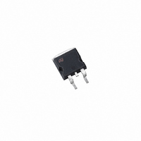
VNB35N07TR-E STMicroelectronics, VNB35N07TR-E Datasheet

VNB35N07TR-E
Specifications of VNB35N07TR-E
Available stocks
Related parts for VNB35N07TR-E
VNB35N07TR-E Summary of contents
Page 1
... DESCRIPTION The VNP35N07FI, VNB35N07 and VNV35N07 are monolithic devices made STMicroelectronics VIPower M0 Technology, intended for replacement of standard power MOSFETS KHz applications. Built-in thermal shut-down, linear current limitation and overvoltage clamp protect the chip in harsh BLOCK DIAGRAM ( ) ( ) PowerSO-10 Pin Configuration : INPUT = 6,7,8,9,10; SOURCE = 1,2,4,5; DRAIN = TAB ...
Page 2
VNP35N07FI-VNB35N07-VNV35N07 ABSOLUTE MAXIMUM RATING Symbol Parameter V Drain-source Voltage ( Input Voltage in I Drain Current D I Reverse DC O utput Current R V Electrostatic Discharge (C= 100 pF , R=1 esd P Total ...
Page 3
ELECTRICAL CHARACTERISTICS (continued) SWITCHING ( ) Symb ol Parameter t Turn-on Delay Time d(on) t Rise Time r t Turn-off Delay Time d( Fall T ime f t Turn-on Delay Time d(on) t Rise Time r t Turn-off ...
Page 4
VNP35N07FI-VNB35N07-VNV35N07 PROTECTION FEATURES During normal operation, the Input pin is electrically connected to the gate of the internal power MOSFET. The device then behaves like a standard power MOSFET and can be used as a switch from ...
Page 5
Thermal Impedance For ISOWATT220 Derating Curve Transconductance VNP35N07FI-VNB35N07-VNV35N07 Thermal Impedance For D2PAK / PowerSO-10 Output Characteristics Static Drain-Source On Resistance vs Input Voltage 5/13 ...
Page 6
VNP35N07FI-VNB35N07-VNV35N07 Static Drain-Source On Resistance Input Charge vs Input Voltage Normalized Input Threshold Voltage vs Temperature 6/13 Static Drain-Source On Resistance Capacitance Variations Normalized On Resistance vs Temperature ...
Page 7
Normalized On Resistance vs Temperature Turn-on Current Slope Turn-off Drain-Source Voltage Slope VNP35N07FI-VNB35N07-VNV35N07 Turn-on Current Slope Turn-off Drain-Source Voltage Slope Switching Time Resistive Load 7/13 ...
Page 8
VNP35N07FI-VNB35N07-VNV35N07 Switching Time Resistive Load Current Limit vs Junction Temperature Source Drain Diode Forward Characteristics 8/13 Switching Time Resistive Load Step Response Current Limit ...
Page 9
Fig. 1: Unclamped Inductive Load Test Circuits Fig. 3: Switching Times Test Circuits For Resistive Load Fig. 5: Test Circuit For Inductive Load Switching And Diode Recovery Times VNP35N07FI-VNB35N07-VNV35N07 Fig. 2: Unclamped Inductive Waveforms Fig. 4: Input Charge Test Circuit ...
Page 10
VNP35N07FI-VNB35N07-VNV35N07 ISOWATT220 MECHANICAL DATA DIM. MIN. TYP. A 4.4 B 2.5 D 2.5 E 0.4 F 0.75 F1 1.15 F2 1.15 G 4. 28.6 L4 9 Ø 3 ¯ 10/13 ...
Page 11
TO-263 (D2PAK) MECHANICAL DATA mm DIM. MIN. TYP. A 4.3 A1 2.49 B 0.7 B2 1.25 C 0.45 C2 1. 1. VNP35N07FI-VNB35N07-VNV35N07 MAX. ...
Page 12
VNP35N07FI-VNB35N07-VNV35N07 PowerSO-10 MECHANICAL DATA DIM. MIN. TYP. A 3.35 A1 0.00 B 0.40 c 0.35 D 9.40 D1 7.40 E 9.30 E1 7.20 E2 7.20 E3 6.10 E4 5.90 e 1.27 F 1.25 H 13.80 h 0.50 L 1.20 q ...
Page 13
... STMicroelectronics. Specification mentioned in this publication are subject to change without notice. This publication supersedes and replaces all information previously supplied. STMicroelectronics products are not authorized for use as critical compone nts in life support devices or systems without express written approval of STMicroelectronics. The ST logo is a trademark of STMicroelectronics 1998 STMicroelectronics – ...


