VNP49N04-E STMicroelectronics, VNP49N04-E Datasheet - Page 3
VNP49N04-E
Manufacturer Part Number
VNP49N04-E
Description
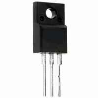
MOSFET POWER 42V 49A TO-220-3
Manufacturer
STMicroelectronics
Series
OMNIFET™r
Type
Low Sider
Datasheet
1.VNP49N04-E.pdf
(11 pages)
Specifications of VNP49N04-E
Input Type
Non-Inverting
Number Of Outputs
1
On-state Resistance
20 mOhm
Current - Peak Output
49A
Mounting Type
Through Hole
Package / Case
TO-220-3 (Straight Leads)
Transistor Polarity
N-Channel
Resistance Drain-source Rds (on)
0.02 Ohms
Forward Transconductance Gfs (max / Min)
30 S
Drain-source Breakdown Voltage
42 V
Continuous Drain Current
49 A
Power Dissipation
125000 mW
Mounting Style
Through Hole
Lead Free Status / RoHS Status
Lead free / RoHS Compliant
Voltage - Supply
-
Operating Temperature
-
Current - Output / Channel
-
Lead Free Status / Rohs Status
Lead free / RoHS Compliant
Available stocks
Company
Part Number
Manufacturer
Quantity
Price
Company:

Part Number:
VNP49N04-E
Manufacturer:
ST
Quantity:
5 000


ELECTRICAL CHARACTERISTICS (continued)
SWITCHING (**)
SOURCE DRAIN DIODE
PROTECTION
(*) Pulsed: Pulse duration = 300 ms, duty cycle 1.5 %
(**) Parameters guaranteed by design/characterization
I
t
Symb ol
Symb ol
Symb ol
T
(di/dt)
T
E
Q
RRM
V
dl im
t
I
jsh
gf
r r
j rs
t
t
as
t
t
SD
r r
d(on)
d(of f)
d(on)
d(of f)
I
Q
lim
t
t
t
t
(**)
(**)
r
f
r
f
(**)
(**)
(**)
(**)
(**)
i
(**)
(*)
on
Turn-on Delay Time
Rise Time
Turn-off Delay Time
Fall T ime
Turn-on Delay Time
Rise Time
Turn-off Delay Time
Fall T ime
Turn-on Current Slope
Total Input Charge
Forward O n Voltage
Reverse Recovery
Time
Reverse Recovery
Charge
Reverse Recovery
Current
Drain Current Limit
Step Response
Current Limit
Overtemperature
Shutdown
Overtemperature Reset
Fault Sink Current
Single Pulse
Avalanche Energy
Parameter
Parameter
Parameter
V
V
(see figure 3)
V
V
(see figure 3)
V
V
V
I
I
V
(see test circuit, figure 5)
V
V
V
V
V
V
starting T
V
SD
SD
DD
gen
DD
gen
DD
i n
DD
DD
i n
i n
i n
i n
i n
i n
i n
= 25 A
= 10 V
= 25 A
= 10 V
= 5 V
= 10 V
= 5 V
= 10 V
= 5 V
= 10 V R
= 15 V
= 15 V
= 15 V
= 15 V
= 30 V
= 10 V
= 10 V
j
Test Cond ition s
Test Cond ition s
Test Cond ition s
= 25
V
V
V
V
V
gen
I
di/dt = 100 A/ms
DS
DS
D
in
DS
DS
T
R
I
D
j
o
R
R
= 25 A
I
I
= 0
gen
C
d
d
= 25
= 13 V
= 13 V
= 1 KW
= 25 A
= 13 V
= 13 V
gen
gen
= 25 A
= 25 A
= 10 W
= 10 W
= 1000 W
V
o
C
DD
V
= 20 V
L = 6 mH
i n
= 10 V
Min.
Min.
Min.
150
135
30
30
4
Typ .
1300
Typ .
Typ .
200
800
300
100
250
910
1.3
3.8
6.1
7.5
12
25
49
49
35
90
50
20
Max.
Max.
Max.
1800
1200
300
450
150
1.9
5.2
8.5
1.6
14
68
68
50
VNP49N04
Un it
Un it
Un it
A/ms
mA
mA
nC
nC
o
o
ns
ns
ns
ns
ms
ms
ms
ms
ns
ms
ms
V
A
A
A
J
C
C
3/11
Related parts for VNP49N04-E
Image
Part Number
Description
Manufacturer
Datasheet
Request
R

Part Number:
Description:
STMicroelectronics [RIPPLE-CARRY BINARY COUNTER/DIVIDERS]
Manufacturer:
STMicroelectronics
Datasheet:
Part Number:
Description:
STMicroelectronics [LIQUID-CRYSTAL DISPLAY DRIVERS]
Manufacturer:
STMicroelectronics
Datasheet:

Part Number:
Description:
BOARD EVAL FOR MEMS SENSORS
Manufacturer:
STMicroelectronics
Datasheet:
Part Number:
Description:
NPN TRANSISTOR POWER MODULE
Manufacturer:
STMicroelectronics
Datasheet:
Part Number:
Description:
TURBOSWITCH ULTRA-FAST HIGH VOLTAGE DIODE
Manufacturer:
STMicroelectronics
Datasheet:
Part Number:
Description:
Manufacturer:
STMicroelectronics
Datasheet:
Part Number:
Description:
DIODE / SCR MODULE
Manufacturer:
STMicroelectronics
Datasheet:
Part Number:
Description:
DIODE / SCR MODULE
Manufacturer:
STMicroelectronics
Datasheet:
Part Number:
Description:
Search -----> STE16N100
Manufacturer:
STMicroelectronics
Datasheet:
Part Number:
Description:
Search ---> STE53NA50
Manufacturer:
STMicroelectronics
Datasheet:
Part Number:
Description:
NPN Transistor Power Module
Manufacturer:
STMicroelectronics
Datasheet:
Part Number:
Description:
DIODE / SCR MODULE
Manufacturer:
STMicroelectronics
Datasheet: