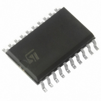
L9826 STMicroelectronics, L9826 Datasheet - Page 8

L9826
Manufacturer Part Number
L9826
Description
IC DRIVER OCTAL LOW SIDE SOIC-20
Manufacturer
STMicroelectronics
Type
Low Sider
Specifications of L9826
Input Type
SPI
Number Of Outputs
8
On-state Resistance
1.5 Ohm
Current - Peak Output
1.1A
Voltage - Supply
4.5 V ~ 5.5 V
Operating Temperature
-40°C ~ 150°C
Mounting Type
Surface Mount
Package / Case
20-SOIC (7.5mm Width)
Supply Voltage (min)
4.5 V
Supply Current
5 mA
Maximum Operating Temperature
+ 150 C
Mounting Style
SMD/SMT
Minimum Operating Temperature
- 40 C
Number Of Drivers
8
Lead Free Status / RoHS Status
Lead free / RoHS Compliant
Current - Output / Channel
-
Lead Free Status / Rohs Status
Lead free / RoHS Compliant
Available stocks
Company
Part Number
Manufacturer
Quantity
Price
Part Number:
L9826TR
Manufacturer:
ST
Quantity:
20 000
3 Electrical Specifications
Table 4.
8/17
I
Outputs short circuit protection
Diagnostics
Outputs timing
Serial diagnostic link (Load capacitor at SDO = 100pF)
Symbol
dU
dU
dU
dU
OUTL1 - 8
R
C
t
t
I
t
V
V
I
t
don1
don2
SBC
SCB
I
DSon
LIM
doff
OUT
t
on1/dt
on2/dt
off1/dt
off2/dt
OL
DG
clp
df
Leakage current
Output clamp voltage
On resistance OUT 1 ... 8
Output capacitance
Overcurrent shutoff threshold
Short circuit current limitation
Delay shutdown
Diagnostic threshold voltage
Open load detection sink
current
Diagnostic detection filter time
Turn ON delay of OUT 1 and 2
Turn ON delay of OUT 3 to 8
Turn OFF delay of OUT 1 to 8
Turn ON voltage slew-rate
Turn ON voltage slew-rate
Turn OFF voltage slew-rate
Turn OFF voltage slew-rate
Electrical Characteristcs (continued)
(4.5V ≤ V
Parameter
CC
≤ 5,5V; -40°C ≤ T
OUTx = OFF; V
V
1mA ≤ I
correlation
I
V
guaranteed by design
OUT3 ... OUT8
OUT1; OUT2
V
for output 1 & 2 on each
diagnostic condition
NON
NCS = 50% to V
(V
NCS = 50% to V
(V
NCS = 50% to V
NON
(V
For output 3 to 8; 90% to 30% of
V
For output 1 and 2; 90% to 30%
of V
For output 1 to 8; 30% to 90% of
V
For output 1 to 8; 30% to 80% of
V
OUT
out
CC
OUT
bat
bat
bat
BAT
BAT
BAT
J
; R
bat
; R
; R
= V
≤ 150°C; unless otherwise specified).
= 1V
= 250mA; T
1, 2
1, 2
= 16V; f = 1MHz
= 16V, R
= 16V, R
= 16V, R
; R
L
L
L
clp
CD00002120
DG
= 500Ω; V
= 500Ω; V
= 500Ω; V
= 50% to V
= 50% to V
Test Condition
L
≤ I
= 500Ω; V
outp
L
L
L
OUTx
; I
OUT
= 500Ω)
OUT
= 500Ω)
OUT
= 500Ω)
j
test
= +150°C
bat
bat
bat
OUT
OUT
= 10mA with
= 0,9·V
= 0,9·V
= 0,1·V
= 16V;
bat
= 16V
= 16V
= 0.9 · V
= 0,9·V
= 0,1·V
= 16V
bat
bat
bat
clp
bat
bat
·V
Min.
0.45
0.32
0.5
0.2
0.7
45
20
15
2
2
2
CC
Typ.
3,0
0.4·V
Max.
300
100
3.5
12
10
62
3.0
1.1
1.1
50
10
10
10
10
15
5
CC
L9826
V/µs
V/µs
V/µs
V/µs
Unit
µA
µA
pF
µs
µs
µs
µs
µs
Ω
V
A
A
V


