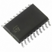
L9826 STMicroelectronics, L9826 Datasheet - Page 10

L9826
Manufacturer Part Number
L9826
Description
IC DRIVER OCTAL LOW SIDE SOIC-20
Manufacturer
STMicroelectronics
Type
Low Sider
Specifications of L9826
Input Type
SPI
Number Of Outputs
8
On-state Resistance
1.5 Ohm
Current - Peak Output
1.1A
Voltage - Supply
4.5 V ~ 5.5 V
Operating Temperature
-40°C ~ 150°C
Mounting Type
Surface Mount
Package / Case
20-SOIC (7.5mm Width)
Supply Voltage (min)
4.5 V
Supply Current
5 mA
Maximum Operating Temperature
+ 150 C
Mounting Style
SMD/SMT
Minimum Operating Temperature
- 40 C
Number Of Drivers
8
Lead Free Status / RoHS Status
Lead free / RoHS Compliant
Current - Output / Channel
-
Lead Free Status / Rohs Status
Lead free / RoHS Compliant
Available stocks
Company
Part Number
Manufacturer
Quantity
Price
Part Number:
L9826TR
Manufacturer:
ST
Quantity:
20 000
4 Functional Description
4
4.1
4.2
Figure 4.
10/17
NCS
CLK
SDO
SDI
Functional Description
General
The L9826 integrated circuit features 8 power low-side-driver outputs. Data is transmitted to the
device using the Serial Peripheral Interface, SPI protocol. Outputs 1 and 2 can be controlled
parallel or serial. The power outputs features voltage clamping function for flyback current
recirculation and are protected against short circuit to Vbat.
The diagnostics recognizes two outputs fault conditions: 1) overcurrent for outputs 3 to 8 ,
overcurrent and thermal overload for outputs 1 and 2 in switch-on condition and 2) open load
or short to GND in switch-off condition for all outputs. The outputs status can be read out via
the serial interface.
The chip internal reset is a OR function of the external nRes signal and internally generated
undervoltage nRes signal.
Output Stages Control
Each output is controlled with its latch and with common reset line, which enables all eight
outputs. Outputs 1 and 2 can be controlled also by its NON1, NON2 inputs. It allows PWM
control independently on the SPI. These inputs features internal pull-up resistors to assure that
the outputs are switched off, when the inputs are open.
The control data are transmitted via the SDI input, the timing of the serial interface is shown in
Figure
The device is selected with low NCS signal and the input data are transferred into the 8 bit shift
register at every falling CLK edge. The rising edge of the NCS latches the new data from the
shift register to the drivers.
The SPI register data are transferred to the output latch at rising NCS edge. The digital filter
between NCS and the output latch ensures that the data are transferred only after 8 CLK cycles
or multiple of 8 CLK cycles since the last NCS falling edge. The NCS changes only at low CLK.
Timing of the Serial Interface
tsclch
tcsdv
4..
thclcl
not defined
tpcld
tscld
tclh
D8
D8
thcld
CD00002120
tcll
D7
D1
tsclcl
D1
tpchdz
thclch
L9826


