ATA6829-T3QY 71 Atmel, ATA6829-T3QY 71 Datasheet - Page 7
ATA6829-T3QY 71
Manufacturer Part Number
ATA6829-T3QY 71
Description
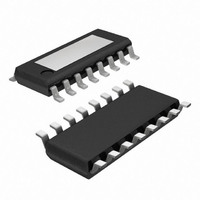
IC DRIVER TRPL HALFBRIDGE 16PSOP
Manufacturer
Atmel
Type
High Side/Low Side Driverr
Datasheet
1.ATA6829-T3QY_71.pdf
(16 pages)
Specifications of ATA6829-T3QY 71
Input Type
Serial
Number Of Outputs
6
On-state Resistance
1.1 Ohm
Current - Peak Output
2A
Voltage - Supply
5.6 V ~ 40 V
Operating Temperature
-40°C ~ 150°C
Mounting Type
Surface Mount
Package / Case
16-PSOP
Product
Half-Bridge Drivers
Rise Time
100 ns
Fall Time
100 ns
Supply Voltage (max)
40 V
Supply Current
350 uA
Maximum Operating Temperature
+ 150 C
Mounting Style
SMD/SMT
Minimum Operating Temperature
- 55 C
Number Of Drivers
3
Output Current
- 10 A to + 10 A
Output Voltage
40 V
Lead Free Status / RoHS Status
Lead free / RoHS Compliant
Current - Output / Channel
-
Lead Free Status / Rohs Status
Lead free / RoHS Compliant


4. Absolute Maximum Ratings
Stresses beyond those listed under “Absolute Maximum Ratings” may cause permanent damage to the device. This is a stress rating
only and functional operation of the device at these or any other conditions beyond those indicated in the operational sections of this
specification is not implied. Exposure to absolute maximum rating conditions for extended periods may affect device reliability.
All values refer to GND pins.
5. Thermal Resistance
6. Operating Range
Note:
4531G–BCD–07/09
Parameters
Supply voltage
Supply voltage
t < 0.5s; I
Logic supply voltage
Logic input voltage
Logic output voltage
Input current
Output current
Output current
Output voltage
Reverse conducting current
(t
Junction temperature range
Storage temperature range
Parameters
Junction pin
Junction ambient
Parameters
Supply voltage
Logic supply voltage
Logic input voltage
Serial interface clock frequency
PWM input frequency
Junction temperature range
pulse
= 150 µs)
1. Threshold for undervoltage detection.
S
> –2A
towards pin 12
Test Conditions
Measured to heat slug
GND pins 1, 9 and 16
13 to 15
13 to 15
13 to 15
5 to 8
5 to 8
2 to 4
2 to 4
2 to 4
Pin
12
12
11
10
10
V
CS
V
I
I
I
CS
I
I
I
I
Out3H
Out3H
Out3H
,V
Out3L
Out3L
Out3L
CS
, V
Symbol
DI
, I
V
, V
f
Symbol
V
f
DI
DI
, I
, I
, I
PWM
, I
, I
, I
CLK
VCC
T
V
T
VS
, V
, I
V
V
V
Out2H,
Out2H,
Out2H,
CLK
Out2L,
Out2L,
Out2L,
I
j
T
VCC
DO
STG
DO
VS
VS
CLK
J
CLK
, V
, I
, V
I
I
I
I
I
I
PWM
Out1L
Out1L
Out1L
Out1H
Out1H
Out1H
PWM
PWM
Internally limited, see output specification
Symbol
R
R
thJP
thJA
–0.3 to V
–0.3 to V
–0.3 to V
4.75 to 5.25
–40 to +150
–40 to +150
–55 to +150
V
–0.3 to +40
–0.3 to +40
–10 to +10
–10 to +10
–0.3 to +7
UV
Value
Value
(1)
–1
17
2
1
VCC
VCC
to 40
VCC
+ 0.3
+ 0.3
Value
30
5
ATA6829
MHz
Unit
Unit
K/W
K/W
kHz
Unit
mA
mA
°C
°C
°C
V
V
V
V
V
V
V
V
V
A
7
Related parts for ATA6829-T3QY 71
Image
Part Number
Description
Manufacturer
Datasheet
Request
R

Part Number:
Description:
IC DRIVER TRPL HALFBRIDGE 16PSOP
Manufacturer:
Atmel
Datasheet:

Part Number:
Description:
Dual Triple DMOS Output Driver with Serial Input Control
Manufacturer:
ATMEL Corporation
Datasheet:
Part Number:
Description:
MOSFET & Power Driver ICs Triple Half-Bridge Driver
Manufacturer:
Atmel
Datasheet:

Part Number:
Description:
DEV KIT FOR AVR/AVR32
Manufacturer:
Atmel
Datasheet:
Part Number:
Description:
INTERVAL AND WIPE/WASH WIPER CONTROL IC WITH DELAY
Manufacturer:
ATMEL Corporation
Datasheet:
Part Number:
Description:
Low-Voltage Voice-Switched IC for Hands-Free Operation
Manufacturer:
ATMEL Corporation
Datasheet:
Part Number:
Description:
MONOLITHIC INTEGRATED FEATUREPHONE CIRCUIT
Manufacturer:
ATMEL Corporation
Datasheet:
Part Number:
Description:
AM-FM Receiver IC U4255BM-M
Manufacturer:
ATMEL Corporation
Datasheet:
Part Number:
Description:
Monolithic Integrated Feature Phone Circuit
Manufacturer:
ATMEL Corporation
Datasheet:
Part Number:
Description:
Multistandard Video-IF and Quasi Parallel Sound Processing
Manufacturer:
ATMEL Corporation
Datasheet:
Part Number:
Description:
High-performance EE PLD
Manufacturer:
ATMEL Corporation
Datasheet:
Part Number:
Description:
8-bit Flash Microcontroller
Manufacturer:
ATMEL Corporation
Datasheet: