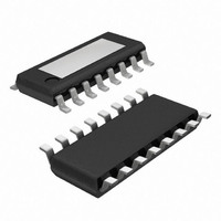
ATA6829-T3QY 71 Atmel, ATA6829-T3QY 71 Datasheet - Page 13

ATA6829-T3QY 71
Manufacturer Part Number
ATA6829-T3QY 71
Description
IC DRIVER TRPL HALFBRIDGE 16PSOP
Manufacturer
Atmel
Type
High Side/Low Side Driverr
Datasheet
1.ATA6829-T3QY_71.pdf
(16 pages)
Specifications of ATA6829-T3QY 71
Input Type
Serial
Number Of Outputs
6
On-state Resistance
1.1 Ohm
Current - Peak Output
2A
Voltage - Supply
5.6 V ~ 40 V
Operating Temperature
-40°C ~ 150°C
Mounting Type
Surface Mount
Package / Case
16-PSOP
Product
Half-Bridge Drivers
Rise Time
100 ns
Fall Time
100 ns
Supply Voltage (max)
40 V
Supply Current
350 uA
Maximum Operating Temperature
+ 150 C
Mounting Style
SMD/SMT
Minimum Operating Temperature
- 55 C
Number Of Drivers
3
Output Current
- 10 A to + 10 A
Output Voltage
40 V
Lead Free Status / RoHS Status
Lead free / RoHS Compliant
Current - Output / Channel
-
Lead Free Status / Rohs Status
Lead free / RoHS Compliant
10. Application Circuit
10.1
4531G–BCD–07/09
Application Notes
Watchdog
U5021M
V
CC
V
CC
It is strongly recommended to connect the blocking capacitors at V
ble to the power supply and GND pins.
Recommended value for capacitors at V
Electrolytic capacitor C > 22 µF in parallel with a ceramic capacitor C = 100 nF. Value for elec-
trolytic capacitor depends on external loads, conducted interferences and reverse conducting
current I
Recommended value for capacitors at V
Electrolytic capacitor C > 10 µF in parallel with a ceramic capacitor C = 100 nF.
To reduce thermal resistance it is recommended to place cooling areas on the PCB as close as
possible to the GND pins. Negative spikes at the output pins (e.g. negative spikes caused by an
inductive load switched off with a high side driver) may activate the overtemperature protection
function of the ATA6829. In this condition, the affected output will be switched off. If this behavior
is not acceptable or compatible with the specific application functionally, it is necessary, that for
switching on required outputs again, the SRR bit (Status Register Reset) is set, to ensure a reset
of the overtemperature function.
PWM
CLK
DO
CS
DI
10
6
7
5
8
Out1,2,3
S
P
S
F
I
OUT3H
OUT3L
H
detect
O
C
S
N
I
Fault
Input register
detect
Fault
(see
Output register
O
O
V
L
D
L
4
3
P
H
3
n.
u.
“Absolute Maximum Ratings” on page
P
L
3
n.
u.
P
H
2
n.
u.
M
P
L
2
n.
u.
OUT2H
OUT2L
P
H
1
n.
u.
detect
Fault
detect
Fault
P
L
1
n.
u.
14
15
H
S
3
H
S
3
Serial interface
S
L
3
S
L
3
H
S
2
H
S
2
M
L
S
2
S
L
2
S
CC
OUT1L
OUT1H
:
H
S
1
H
S
1
detect
detect
Fault
Fault
:
S
L
1
S
L
1
13
2
S
R
R
T
P
Control
logic
protection
Thermal
7).
Charge
pump
protection
Power-on
UV -
reset
CC
and V
11
16
12
1
9
VCC
GND
GND
GND
VS
S
as close as possi-
ATA6829
V
+ +
S
+
0 to 40 V
V
Batt
V
5 V
CC
13


