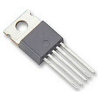
BTS555 Infineon Technologies, BTS555 Datasheet - Page 10

BTS555
Manufacturer Part Number
BTS555
Description
IC HISIDE PWR SWTCH TO218AB/5-1
Manufacturer
Infineon Technologies
Series
PROFET®r
Type
High Sider
Specifications of BTS555
Input Type
Non-Inverting
Number Of Outputs
1
On-state Resistance
1.9 mOhm
Current - Output / Channel
165A
Current - Peak Output
520A
Voltage - Supply
5 V ~ 34 V
Operating Temperature
-40°C ~ 150°C
Mounting Type
Through Hole
Package / Case
TO-218AB/5
Module Configuration
High Side
Peak Output Current
165A
Output Resistance
1.9ohm
Input Delay
600µs
Output Delay
200µs
Supply Voltage Range
5V To 34V
Driver Case Style
TO-218AB
No. Of Pins
5
Operating Temperature Range
-40°C To +150°C
Rohs Compliant
No
Device Type
High Side
Lead Free Status / RoHS Status
Contains lead / RoHS non-compliant
Other names
BTS555NK
SP000011266
SP000011266
Available stocks
Company
Part Number
Manufacturer
Quantity
Price
Company:
Part Number:
BTS555
Manufacturer:
INFINEON
Quantity:
3 000
Part Number:
BTS555
Manufacturer:
INFINEON/英飞凌
Quantity:
20 000
Company:
Part Number:
BTS555E3146HKSA1
Manufacturer:
INFINEON
Quantity:
12 000
Inverse load current operation
The device is specified for inverse load current
operation (V
is not available during this kind of operation (I
With I
source diode is conducting resulting in considerably
increased power dissipation. If the device is switched
on (V
much lower value R
4).
Note: Temperature protection during inverse load
current operation is not possible!
Inductive load switch-off energy
dissipation
Energy stored in load inductance:
While demagnetizing load inductance, the energy
dissipated in PROFET is
with an approximate solution for R L
Infineon Technologies AG
+
-
E
V bb
AS
IN
IN
= 0), this power dissipation is decreased to the
=
= 0 (e.g. input open) only the intrinsic drain
E
I
E
V
IN
V
bb
2
I
AS
bb
L
IN
·
R
·
OUT
L
= E
L
(
V
bb
> V
bb
IN
+ E
ON(INV)
+ |V
bb
E
IN
V
L
L
> 0V). The current sense feature
IS
PROFET
OUT(CL)
- E
=
IS
V
1 /
R
PROFET
* I
bb
2
=
·
R IS
V
IS
2
∫
bb
L
(specifications see page
|)
·
V
I
R
IS
ON(CL)
I
OUT
2
L
ln
IS
(1+
OUT
E AS
Z L
0 :
·
|V
{
i
L
i (t)
L
(t) dt,
OUT(CL)
R L
I
L
L
·
V
- I
IS
R
OUT
L
L
= 0).
E
|
E
E Load
R
)
+
L
-
10
Maximum allowable load inductance for
a single switch off
L = f (I L ); T j,start = 150°C, V bb = 12 V, R L = 0
L [µH]
Externally adjustable current limit
If the device is conducting, the sense current can be
used to reduce the short circuit current and allow
higher lead inductance (see diagram above). The
device will be turned off, if the threshold voltage of T2
is reached by I
R
the short circuit current is defined by I
device is shut down after t
IN
Signal
V
1000000
*C
100000
10000
V
1000
T1 will be reset. The device is turned on again,
100
10
Signal
GND
1
R
V
1
T1
V bb
S
*R
IS
. After a delay time defined by
IN
C
10
V
d(SC)
Data Sheet BTS555
PROFET
T2
V bb
with latch function.
100
OUT
L(SC)
IS
2008-June-24
R
and the
IS
R
Power
GND
1000
load
I L [A]


