VND600SP STMicroelectronics, VND600SP Datasheet - Page 6
VND600SP
Manufacturer Part Number
VND600SP
Description
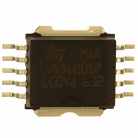
IC DRIVER DUAL 36V 25A PWRSO-10
Manufacturer
STMicroelectronics
Type
High Sider
Datasheet
1.VND600SP13TR.pdf
(26 pages)
Specifications of VND600SP
Input Type
Non-Inverting
Number Of Outputs
2
On-state Resistance
30 mOhm
Current - Peak Output
40A
Voltage - Supply
5.5 V ~ 36 V
Operating Temperature
-40°C ~ 150°C
Mounting Type
Surface Mount
Package / Case
PowerSO-10 Exposed Bottom Pad
Switch Type
High Side
Power Switch Family
VND600SP
Power Switch On Resistance
30mOhm
Output Current
25A
Mounting
Surface Mount
Supply Current
6mA
Package Type
PowerSO
Operating Temperature (min)
-40C
Operating Temperature (max)
150C
Operating Temperature Classification
Automotive
Pin Count
12
Power Dissipation
96.1W
Load Current Rating
25 A
Relay Type
Solid State
Termination Style
Solder Leads
Lead Free Status / RoHS Status
Contains lead / RoHS non-compliant
Current - Output / Channel
-
Lead Free Status / Rohs Status
Not Compliant
Other names
497-2711-5
Available stocks
Company
Part Number
Manufacturer
Quantity
Price
Company:

Part Number:
VND600SP
Manufacturer:
ST
Quantity:
5 510
Part Number:
VND600SP
Manufacturer:
ST
Quantity:
20 000
Company:
Part Number:
VND600SP-E
Manufacturer:
ST
Quantity:
1 940
Company:
Part Number:
VND600SPTR-E
Manufacturer:
PANASONIC
Quantity:
3 000
Part Number:
VND600SPTR-E
Manufacturer:
ST
Quantity:
20 000


Electrical specifications
2
2.1
6/26
Electrical specifications
Figure 3.
Absolute maximum ratings
Stressing the device above the rating listed in the “Absolute maximum ratings” table may
cause permanent damage to the device. These are stress ratings only and operation of the
device at these or any other conditions above those indicated in the Operating sections of
this specification is not implied. Exposure to Absolute Maximum Rating conditions for
extended periods may affect device reliability. Refer also to the STMicroelectronics SURE
Program and other relevant quality document.
Table 3.
V
Symbol
- I
CSENSE
V
-V
I
V
OUT
I
ESD
GND
I
CC
IN
R
CC
DC supply voltage
Reverse supply voltage
DC reverse ground pin current
Output current
Reverse output current
Input current
Current sense maximum voltage
Electrostatic discharge (human body model: R = 1.5K
C = 100pF)
- INPUT
- CURRENT SENSE
- OUTPUT
- V
Current and voltage conventions
V
Absolute maximum ratings
CC
IN1
V
IN2
I
I
IN2
IN1
INPUT1
INPUT2
Parameter
CURRENT SENSE 2
CURRENT SENSE 1
GROUND
OUTPUT2
OUTPUT1
I
GND
V
CC
V
SENSE2
I
I
I
I
OUT1
SENSE2
SENSE1
OUT2
V
OUT2
V
V
F1
SENSE1
I
S
(*)
Internally limited
V
OUT1
Value
+/- 10
- 200
4000
2000
5000
5000
- 0.3
+ 15
- 21
41
- 3
VND600SP
V
CC
Unit
mA
mA
V
V
A
A
V
V
V
V
V
V
Related parts for VND600SP
Image
Part Number
Description
Manufacturer
Datasheet
Request
R

Part Number:
Description:
RELAY SSR 2CHAN HI SIDE 16SOIC
Manufacturer:
STMicroelectronics
Datasheet:

Part Number:
Description:
IC DVR HIGH SIDE 2CH 25A 16SOIC
Manufacturer:
STMicroelectronics
Datasheet:
Part Number:
Description:
STMicroelectronics [RIPPLE-CARRY BINARY COUNTER/DIVIDERS]
Manufacturer:
STMicroelectronics
Datasheet:
Part Number:
Description:
STMicroelectronics [LIQUID-CRYSTAL DISPLAY DRIVERS]
Manufacturer:
STMicroelectronics
Datasheet:

Part Number:
Description:
BOARD EVAL FOR MEMS SENSORS
Manufacturer:
STMicroelectronics
Datasheet:
Part Number:
Description:
NPN TRANSISTOR POWER MODULE
Manufacturer:
STMicroelectronics
Datasheet:
Part Number:
Description:
TURBOSWITCH ULTRA-FAST HIGH VOLTAGE DIODE
Manufacturer:
STMicroelectronics
Datasheet:
Part Number:
Description:
Manufacturer:
STMicroelectronics
Datasheet:
Part Number:
Description:
DIODE / SCR MODULE
Manufacturer:
STMicroelectronics
Datasheet:
Part Number:
Description:
DIODE / SCR MODULE
Manufacturer:
STMicroelectronics
Datasheet:
Part Number:
Description:
Search -----> STE16N100
Manufacturer:
STMicroelectronics
Datasheet:
Part Number:
Description:
Search ---> STE53NA50
Manufacturer:
STMicroelectronics
Datasheet: