VND830ASP13TR STMicroelectronics, VND830ASP13TR Datasheet - Page 8
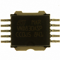
VND830ASP13TR
Manufacturer Part Number
VND830ASP13TR
Description
IC DRIVER 2CHAN HI SIDE PWR SO10
Manufacturer
STMicroelectronics
Type
High Sider
Datasheet
1.VND830ASP13TR.pdf
(17 pages)
Specifications of VND830ASP13TR
Input Type
Non-Inverting
Number Of Outputs
2
On-state Resistance
60 mOhm
Current - Peak Output
10A
Voltage - Supply
5.5 V ~ 36 V
Operating Temperature
-40°C ~ 150°C
Mounting Type
Surface Mount
Package / Case
PowerSO-10 Exposed Bottom Pad
Load Current Rating
25 A
Relay Type
Double Channel High Side Solid State Relay
Lead Free Status / RoHS Status
Contains lead / RoHS non-compliant
Current - Output / Channel
-
Lead Free Status / Rohs Status
Lead free / RoHS Compliant
Other names
497-4499-2
Available stocks
Company
Part Number
Manufacturer
Quantity
Price
Company:

Part Number:
VND830ASP13TR
Manufacturer:
ST
Quantity:
2 150


GND
REVERSE BATTERY
Solution 1: Resistor in the ground line (R
can be used with any type of load.
The following is an indication on how to dimension the
R
where -I
be found in the absolute maximum rating section of the
device’s datasheet.
Power Dissipation in R
battery situations) is:
P
This resistor can be shared amongst several different
HSD. Please note that the value of this resistor should be
calculated with formula (1) where I
sum of the maximum on-state currents of the different
devices.
Please note that if the microprocessor ground is not
common with the device ground then the R
produce a shift (I
and the status output values. This shift will vary
depending on how many devices are ON in the case of
several high side drivers sharing the same R
VND830ASP
APPLICATION SCHEMATIC
8/17
D
GND
1) R
2) R
= (-V
resistor.
GND
GND
CC
GND
PROTECTION
+5V
)
2
C
/R
600mV / I
is the DC reverse ground pin current and can
GND
V
CC
S(on)max
R
) / (-I
SENSE1
R
R
R
R
prot
prot
prot
S(on)max
prot
GND
GND
* R
)
(when V
NETWORK
GND
.
) in the input thresholds
R
S(on)max
SENSE2
CC
<0: during reverse
CURRENT SENSE2
CURRENT SENSE1
INPUT2
INPUT1
GND
becomes the
GND
AGAINST
only). This
.
GND
will
V
GND
If the calculated power dissipation leads to a large resistor
or several devices have to share the same resistor then
the ST suggests to utilize Solution 2 (see below).
Solution 2: A diode (D
A resistor (R
D
This small signal diode can be safely shared amongst
several different HSDs. Also in this case, the presence of
the ground network will produce a shift (
input thresholds and the status output values if the
microprocessor ground is not common with the device
ground. This shift will not vary if more than one HSD
shares the same diode/resistor network.
Series resistor in INPUT line is also required to prevent
that, during battery voltage transient, the current exceeds
the Absolute Maximum Rating.
Safest configuration for unused INPUT pin is to leave it
unconnected, while unused SENSE pin has to be
connected to Ground pin.
LOAD DUMP PROTECTION
D
load dump peak voltage exceeds V
same applies if the device will be subject to transients on
the V
ISO T/R 7637/1 table.
GND
ld
GND
R
is necessary (Voltage Transient Suppressor) if the
GND
CC
if the device will be driving an inductive load.
line that are greater than the ones shown in the
V
CC
GND
D
=1k
GND
GND
OUTPUT1
OUTPUT2
should be inserted in parallel to
) in the ground line.
CC
max DC rating. The
j
600mV) in the
D
ld
Related parts for VND830ASP13TR
Image
Part Number
Description
Manufacturer
Datasheet
Request
R

Part Number:
Description:
STMicroelectronics [RIPPLE-CARRY BINARY COUNTER/DIVIDERS]
Manufacturer:
STMicroelectronics
Datasheet:
Part Number:
Description:
STMicroelectronics [LIQUID-CRYSTAL DISPLAY DRIVERS]
Manufacturer:
STMicroelectronics
Datasheet:

Part Number:
Description:
BOARD EVAL FOR MEMS SENSORS
Manufacturer:
STMicroelectronics
Datasheet:
Part Number:
Description:
NPN TRANSISTOR POWER MODULE
Manufacturer:
STMicroelectronics
Datasheet:
Part Number:
Description:
TURBOSWITCH ULTRA-FAST HIGH VOLTAGE DIODE
Manufacturer:
STMicroelectronics
Datasheet:
Part Number:
Description:
Manufacturer:
STMicroelectronics
Datasheet:
Part Number:
Description:
DIODE / SCR MODULE
Manufacturer:
STMicroelectronics
Datasheet:
Part Number:
Description:
DIODE / SCR MODULE
Manufacturer:
STMicroelectronics
Datasheet:
Part Number:
Description:
Search -----> STE16N100
Manufacturer:
STMicroelectronics
Datasheet:
Part Number:
Description:
Search ---> STE53NA50
Manufacturer:
STMicroelectronics
Datasheet:
Part Number:
Description:
NPN Transistor Power Module
Manufacturer:
STMicroelectronics
Datasheet:
Part Number:
Description:
DIODE / SCR MODULE
Manufacturer:
STMicroelectronics
Datasheet: