VND830ASP13TR STMicroelectronics, VND830ASP13TR Datasheet - Page 3
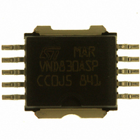
VND830ASP13TR
Manufacturer Part Number
VND830ASP13TR
Description
IC DRIVER 2CHAN HI SIDE PWR SO10
Manufacturer
STMicroelectronics
Type
High Sider
Datasheet
1.VND830ASP13TR.pdf
(17 pages)
Specifications of VND830ASP13TR
Input Type
Non-Inverting
Number Of Outputs
2
On-state Resistance
60 mOhm
Current - Peak Output
10A
Voltage - Supply
5.5 V ~ 36 V
Operating Temperature
-40°C ~ 150°C
Mounting Type
Surface Mount
Package / Case
PowerSO-10 Exposed Bottom Pad
Load Current Rating
25 A
Relay Type
Double Channel High Side Solid State Relay
Lead Free Status / RoHS Status
Contains lead / RoHS non-compliant
Current - Output / Channel
-
Lead Free Status / Rohs Status
Lead free / RoHS Compliant
Other names
497-4499-2
Available stocks
Company
Part Number
Manufacturer
Quantity
Price
Company:

Part Number:
VND830ASP13TR
Manufacturer:
ST
Quantity:
2 150


THERMAL DATA
(*) When mounted on a standard single-sided FR-4 board with 0.5cm
ELECTRICAL CHARACTERISTICS (8V<V
(Per each channel)
POWER OUTPUT
SWITCHING (V
LOGIC INPUT (Channels 1,2)
Note 1: V
dV
dV
Symbol
Symbol
R
Symbol
Symbol
R
flow
V
OUT
OUT
V
I
I
I
I
V
V
thj-case
L(off1)
L(off2)
L(off3)
L(off4)
t
t
thj-amb
R
V
V
I(hyst)
V
clamp
V
d(on)
d(off)
I
I
USD
I
IH
ICL
IL
CC
OV
ON
S
IL
IH
/dt
/dt
clamp
(on)
(off)
and V
Input low level voltage
Low level input current
Input high level voltage
High level input current
Input hysteresis voltage
Input clamp voltage
Thermal Resistance Junction-case
Thermal Resistance Junction-ambient
Operating Supply Voltage
Undervoltage Shut-down
Overvoltage Shut-down
On State Resistance
Clamp voltage
Supply Current
Off State Output Current
Off State Output Current
Off State Output Current
Off State Output Current
Turn-on Delay Time
Turn-off Delay Time
Turn-on Voltage Slope
Turn-off Voltage Slope
OV
CC
Parameter
are correlated. Typical difference is 5V.
Parameter
Parameter
=13V)
Parameter
V
V
I
I
I
I
I
Off State; V
Off State; V
T
On State; V
R
V
V
V
V
R
V
R
V
R
R
IN
IN
OUT
OUT
CC
IN
IN
j
OUT
OUT
IN
IN
IN
IN
L
L
L
L
SENSE
=1mA
=-1mA
=25°C
=6.5 from V
=6.5 from V
=6.5 from V
=6.5 from V
=1.25V
=3.25V
=20 mA (see note 1)
=V
=0V; V
=V
=V
=2A; T
=2A; T
=1.3V
=11.7V
OUT
OUT
OUT
=3.9K
CC
=0V; V
=0V; V
=0V; V
OUT
Test Conditions
<36V; -40°C< T
Test Conditions
j
j
CC
CC
IN
Test Conditions
=25°C
=150°C
=5V; V
=3.5V
=13V; V
=13V; V
OUT
OUT
IN
IN
CC
CC
CC
rising edge to
falling edge to
2
=36V; T
=13V; T
=13V; T
=1.3V to V
=11.7V to V
of Cu (at least 35 m thick). Horizontal mounting and no artificial air
CC
IN=
IN=
=13V; I
V
V
OUT
OUT
j
j
j
=125°C
=125°C
=25°C
j
OUT
OUT
=0V
=0V;
<150°C, unless otherwise specified)
OUT
=0A;
=10.4V
=1.3V
Min
Min
3.25
Min
5.5
-75
0.5
36
41
3
0
1
6
diagram
diagram
51.2 (*)
relative
relative
Value
Typ
Typ
See
See
-0.7
Typ
1.2
6.8
13
48
12
12
30
30
4
VND830ASP
Max
Max
1.25
120
Max
5.5
36
60
55
40
25
50
10
7
0
5
3
8
°C/W
°C/W
Unit
Unit
Unit
Unit
V/ s
V/ s
mA
m
m
V
V
V
V
V
V
V
V
V
A
A
A
A
A
A
A
A
3/17
s
s
1
Related parts for VND830ASP13TR
Image
Part Number
Description
Manufacturer
Datasheet
Request
R

Part Number:
Description:
STMicroelectronics [RIPPLE-CARRY BINARY COUNTER/DIVIDERS]
Manufacturer:
STMicroelectronics
Datasheet:
Part Number:
Description:
STMicroelectronics [LIQUID-CRYSTAL DISPLAY DRIVERS]
Manufacturer:
STMicroelectronics
Datasheet:

Part Number:
Description:
BOARD EVAL FOR MEMS SENSORS
Manufacturer:
STMicroelectronics
Datasheet:
Part Number:
Description:
NPN TRANSISTOR POWER MODULE
Manufacturer:
STMicroelectronics
Datasheet:
Part Number:
Description:
TURBOSWITCH ULTRA-FAST HIGH VOLTAGE DIODE
Manufacturer:
STMicroelectronics
Datasheet:
Part Number:
Description:
Manufacturer:
STMicroelectronics
Datasheet:
Part Number:
Description:
DIODE / SCR MODULE
Manufacturer:
STMicroelectronics
Datasheet:
Part Number:
Description:
DIODE / SCR MODULE
Manufacturer:
STMicroelectronics
Datasheet:
Part Number:
Description:
Search -----> STE16N100
Manufacturer:
STMicroelectronics
Datasheet:
Part Number:
Description:
Search ---> STE53NA50
Manufacturer:
STMicroelectronics
Datasheet:
Part Number:
Description:
NPN Transistor Power Module
Manufacturer:
STMicroelectronics
Datasheet:
Part Number:
Description:
DIODE / SCR MODULE
Manufacturer:
STMicroelectronics
Datasheet: