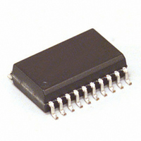
MC33883DW Freescale Semiconductor, MC33883DW Datasheet - Page 12

MC33883DW
Manufacturer Part Number
MC33883DW
Description
IC H-BRIDGE PRE-DRIVER 20-SOIC
Manufacturer
Freescale Semiconductor
Datasheet
1.MCZ33883EGR2.pdf
(21 pages)
Specifications of MC33883DW
Configuration
H Bridge
Input Type
Non-Inverting
Delay Time
200ns
Current - Peak
2A
Number Of Configurations
1
Number Of Outputs
4
Voltage - Supply
5.5 V ~ 55 V
Operating Temperature
-40°C ~ 125°C
Mounting Type
Surface Mount
Package / Case
20-SOIC (7.5mm Width)
Lead Free Status / RoHS Status
Contains lead / RoHS non-compliant
High Side Voltage - Max (bootstrap)
-
Available stocks
Company
Part Number
Manufacturer
Quantity
Price
Part Number:
MC33883DW
Manufacturer:
FAIRCHILD/仙童
Quantity:
20 000
Part Number:
MC33883DWR2
Manufacturer:
FREESCALE
Quantity:
20 000
DRIVER CHARACTERISTICS
gate driver. In the schematic, HSS represents the switch that
is used to charge the external high-side MOSFET through the
GATE_HS terminal. LSS represents the switch that is used to
discharge the external high-side MOSFET through the
GATE_HS terminal. A 180KΩ internal typical passive
discharge resistance and a 18 V typical protection zener are
in parallel with LSS. The same schematic can be applied to
the external low-side MOSFET driver simply by replacing
terminal CP_OUT with terminal LR_OUT, terminal GATE_HS
with terminal GATE_LS, and terminal SRC_HS with GND.
IN_HS1
12
33883
FUNCTIONAL DEVICE OPERATION
Figure 5. High-Side Gate Driver Functional Schematic
Figure 5
represents the external circuit of the high-side
HSSDC_IN
HSSpulse_IN
LSS_IN
HSS
LSS
FUNCTIONAL DEVICE OPERATION
I
I
discharge LSS
charge HSS
18V
180
kΩ
CP_OUT
GATE_HS1
SRC_HS1
I
GATE_HS
driver are illustrated in
peak current of up to 1.0 A for 200 ns to turn on the gate. After
200 ns, 100 mA is continuously provided to maintain the gate
charged. The output driver sinks a high current to turn off the
gate. This current can be up to 1.0 A peak for a 100 nF load.
chronograms. A smaller load will give lower peak and DC charge or
discharge currents.
HSSpulse_IN
I
HSS DC_IN
discharge LSS
The different voltages and current of the high-side gate
Note GATE_HS is loaded with a 100 nF capacitor in the
I
charge HSS
I
GATE_HS
IN_HS1
LSS_IN
Figure 6. High-Side Gate Driver Chronograms
0
0
0
0
0
0
Analog Integrated Circuit Device Data
Figure
1.0 A Peak
1.0 A Peak
6. The output driver sources a
100 mA Typical
100 mA Typical
Freescale Semiconductor
1.0 A Peak
-1.0 A Peak


