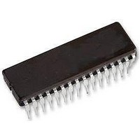
MC33395TDWB Freescale Semiconductor, MC33395TDWB Datasheet - Page 9

MC33395TDWB
Manufacturer Part Number
MC33395TDWB
Description
IC MOSFET PRE-DRVR 3PHASE 32SOIC
Manufacturer
Freescale Semiconductor
Type
3 Phase Brushless DC Motor Controllerr
Datasheet
1.MC33395TEWR2.pdf
(16 pages)
Specifications of MC33395TDWB
Configuration
3 Phase Bridge
Input Type
Non-Inverting
Delay Time
650ns
Number Of Configurations
1
Number Of Outputs
3
Voltage - Supply
5.5 V ~ 24 V
Operating Temperature
-40°C ~ 125°C
Mounting Type
Surface Mount
Package / Case
32-SOIC (7.5mm Width)
Operating Supply Voltage
- 0.3 V to + 7 V
Supply Current
1.8 mA
Mounting Style
SMD/SMT
Lead Free Status / RoHS Status
Contains lead / RoHS non-compliant
Current - Peak
-
High Side Voltage - Max (bootstrap)
-
the necessary drive and control signal buffering and
amplification to enable a DSP or MCU to control a three-
phase array of power MOSFETs such as would be required
to energize the windings of powerful brushless DC (BLDC)
CHARGE PUMP CAPACITOR (CP2H)
capacitor
CHARGE PUMP RESERVE CAPACITOR (CPRES)
INPUT VOLTAGE (VIGN)
HIGH-SIDE GATE VOLTAGE (VGDH)
MOSFET switch
INPUT VOLTAGE PROTECTED (VIGNP)
functions
HIGH-SIDE SENSE (SRC1, SRC2, SRC3)
GATE DRIVE HIGH (GDH1, GDH2, GDH3)
OUTPUT FOR GATE (GDL1, GDL2, GDL3)
POWER GROUND (PGND)
TEST PIN (TEST)
Analog Integrated Circuit Device Data
Freescale Semiconductor
The 33395 and 33395T devices are designed to provide
High potential pin connection for secondary charge pump
Input from external reservoir capacitor for charge pump
Input from ignition level supply voltage for power functions
Output full-time gate drive for auxiliary high-side power
Input from protected ignition level supply for power
Sense for high-side source voltage, phase 1/2/3
Output for gate high-side, phase 1/2/3
Output for gate drive low-side, phase 1
Ground pins for power functions
This should be connected to ground or left open
FUNCTIONAL DESCRIPTION
FUNCTIONAL PIN DESCRIPTION
INTRODUCTION
motors. It contains built-in charge pump circuitry so that the
MOSFET array may consist entirely of N-Channel
MOSFETs. It also contains feedback sensing circuitry and
control circuitry to provide a robust overall motor control
design.
IS MINUS (-ISENS)
IS PLUS (+ISENS)
ANALOG GROUND (AGND)
LOGIC SUPPLY VOLTAGE (VDD)
PULSE WIDTH MODULATOR (PWM)
MODE CONTROL BIT 1 (MODE1)
MODE CONTROL BIT 0 (MODE0)
HIGH-SIDE ENABLE (HSE3, HSE2, HSE1)
LOW-SIDE ENABLE (LSE3, LSE2, LSE1)
EXTERNAL PUMP CAPACITOR (CP1L, CP1H)
secondary pins
CHARGE PUMP CAPACITOR (CP2L)
charge pump, and secondary pins
Inverting input for current limit comparator
Non-Inverting input for current limit comparator
Ground pin for logic functions
Supply voltage for logic functions
Input for pulse width modulated driver duty cycle
Input for mode control selection
Input for mode control selection
Input for high-side enable logic, phase 1/2/3
Input for low-side enable logic, phase 1/2/3
Input from external pump capacitor for charge pump and
Input from external reservoir, external pump capacitors for
FUNCTIONAL DESCRIPTION
INTRODUCTION
33395
9


