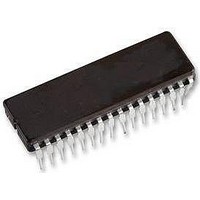
MC33395TDWB Freescale Semiconductor, MC33395TDWB Datasheet - Page 3

MC33395TDWB
Manufacturer Part Number
MC33395TDWB
Description
IC MOSFET PRE-DRVR 3PHASE 32SOIC
Manufacturer
Freescale Semiconductor
Type
3 Phase Brushless DC Motor Controllerr
Datasheet
1.MC33395TEWR2.pdf
(16 pages)
Specifications of MC33395TDWB
Configuration
3 Phase Bridge
Input Type
Non-Inverting
Delay Time
650ns
Number Of Configurations
1
Number Of Outputs
3
Voltage - Supply
5.5 V ~ 24 V
Operating Temperature
-40°C ~ 125°C
Mounting Type
Surface Mount
Package / Case
32-SOIC (7.5mm Width)
Operating Supply Voltage
- 0.3 V to + 7 V
Supply Current
1.8 mA
Mounting Style
SMD/SMT
Lead Free Status / RoHS Status
Contains lead / RoHS non-compliant
Current - Peak
-
High Side Voltage - Max (bootstrap)
-
Table 1. 33395 Pin Definitions
Analog Integrated Circuit Device Data
Freescale Semiconductor
Pin Number
A functional description of each pin can be found in the Functional Pin Description section beginning on
10
11
12
13
14
15
16
17
18
19
20
21
1
2
3
4
5
6
7
8
9
Pin Name
+ISENS
CPRES
-ISENS
VIGNP
VGDH
PGND
AGND
GDH1
GDH2
GDH3
CP2H
SRC1
GDL1
SRC2
SRC3
GDL3
VIGN
PWM
GDL2
VDD
Test
Pin Function
Ground
Ground
Sensor
Sensor
Sensor
Output
Output
Output
Output
Output
Output
Output
Power
Input
Input
Input
Input
Input
Input
N/A
CPRES
VIGNP
VGDH
PGND
GDH1
GDH2
GDH3
Pulse Width Modulator Input for pulse width modulated driver duty cycle
CP2H
SRC1
GDL1
SRC2
GDL2
SRC3
GDL3
TEST
Logic Supply Voltage
VIGN
Charge Pump Cap
High-Side Sense
High-Side Sense
High-Side Sense
Gate Drive High
Gate Drive High
Gate Drive High
High-Side Gate
Output for Gate
Output for Gate
Gate Drive Low
Analog Ground
Formal Name
Power Ground
Charge Pump
Input Voltage
Input Voltage
Reserve Cap
Protected
Figure 3. 33395 Pin Connections
IS Minus
Test Pin
Voltage
IS Plus
PIN CONNECTIONS
1
2
3
4
5
6
7
8
9
10
11
12
13
14
15
16
High potential pin connection for secondary charge pump capacitor
Input from external reservoir capacitor for charge pump
Input from ignition level supply voltage for power functions
Output full-time gate drive for auxiliary high-side power MOSFET switch
Input from protected ignition level supply for power functions
Sense for high-side source voltage, phase 1
Output for gate high-side, phase 1
Output for gate drive low-side, phase 1
Sense for high-side source voltage, phase 2
Output for gate high-side, phase 2
Output for gate drive low-side, phase 2
Sense for high-side source voltage, phase 3
Output for gate drive high-side, phase 3
Output for gate drive low-side, phase 3
Ground pins for power functions
This should be connected to ground or left open
Inverting input for current limit comparator
Non-inverting input for current limit comparator
Ground pin for logic functions
Supply voltage for logic functions
32
31
30
29
28
27
26
25
24
23
22
21
20
19
18
17
CP2L
CP1H
CP1L
LSE1
LSE2
LSE3
HSE1
HSE2
HSE3
MODE0
MODE1
PWM
VDD
AGND
+ISENS
-ISENS
Definition
page
PIN CONNECTIONS
9.
33395
3


