IRS26302DJPBF International Rectifier, IRS26302DJPBF Datasheet - Page 6
IRS26302DJPBF
Manufacturer Part Number
IRS26302DJPBF
Description
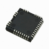
IC BRIDGE +1 GATE DVR 3PH 44PLCC
Manufacturer
International Rectifier
Datasheet
1.IRS26302DJTRPBF.pdf
(51 pages)
Specifications of IRS26302DJPBF
Configuration
3 Phase Bridge
Input Type
Non-Inverting
Delay Time
320ns
Current - Peak
200mA
Number Of Configurations
1
Number Of Outputs
3
High Side Voltage - Max (bootstrap)
600V
Voltage - Supply
10 V ~ 20 V
Operating Temperature
-40°C ~ 125°C
Mounting Type
Surface Mount
Package / Case
44-PLCC (32 Leads)
Number Of Drivers
6
Driver Configuration
Non-Inverting
Driver Type
High and Low Side
Input Logic Level
CMOS/TTL
Rise Time
190ns
Fall Time
75ns
Propagation Delay Time
710ns
Peak Output Current
350mA
Power Dissipation
4.6W
Operating Supply Voltage (min)
10V
Turn Off Delay Time
50ns
Turn On Delay Time (max)
50ns
Operating Temp Range
-40C to 125C
Operating Temperature Classification
Automotive
Mounting
Surface Mount
Pin Count
32
Package Type
PLCC
Lead Free Status / RoHS Status
Lead free / RoHS Compliant
Available stocks
Company
Part Number
Manufacturer
Quantity
Price
Company:

Part Number:
IRS26302DJPBF
Manufacturer:
International Rectifier
Quantity:
10 000


Absolute Maximum Ratings
Absolute maximum ratings indicate sustained limits beyond which damage to the device may occur. All voltage
parameters are absolute voltages referenced to V
power dissipation ratings are measured under board mounted and still air conditions. Voltage clamps are included
between V
V
†
www.irf.com
PFCtrip
Symbol
V
V
VSDC
V
V
dV/dt
R
COM
VDC
HO1,2,3
LO1,2,3
V
GF
V
B1,2,3
S1,2,3
P
T
THJA
T
T
CC
All supplies are fully tested at 25 V. An internal 20 V clamp exists for each supply.
IN
/V
D
S
L
J
BRtrip
CC
& COM (25 V), V
High side floating supply voltage
High side floating output voltage
High side offset voltage
DCbus Supply Voltage
Input voltage for Ground Fault detection
High voltage return for Ground Fault circuit
Low side and logic fixed supply voltage
Power ground
Low side output voltage LO1,2,3, PFCout
Input voltage LIN1,2,3, HIN1,2,3, ITRIP, PFCtrip,
FLTEN, RCIN
Input voltage V
Allowable offset voltage slew rate
Package power dissipation @ TA
Thermal resistance, junction to ambient
Junction temperature
Storage temperature
Lead temperature (soldering, 10 seconds)
CC
PFCtrip
& V
/V
SS
BRtrip
Definition
(20 V), and V
SS
+25° C
unless otherwise stated in the table. The thermal resistance and
B
& V
S
6
(20 V).
V
V
V
VDC-20
VDC-20
S1,2,3
B1,2,3
CC
Min.
-0.3
-0.3
-0.3
-0.3
-0.3
-55
-2
—
—
—
—
—
- 25
- 0.3
- 20
V
V
© 2009 International Rectifier
B 1,2,3
VDC+0.3
VDC+0.3
V
V
V
V
B1,2,3
CC
CC
CC
CC
Max.
IRS26302DJ
620
620
20
150
150
300
4.6
50
27
+ 0.3
+ 0.3
+ 0.3
+ 0.3
†
+ 0.3
+ 0.3
Units
° C/W
V/ns
° C
W
V
Related parts for IRS26302DJPBF
Image
Part Number
Description
Manufacturer
Datasheet
Request
R

Part Number:
Description:
SCHOTTKY RECTIFIER
Manufacturer:
International Rectifier Corp.
Datasheet:
Part Number:
Description:
SCHOTTKY RECTIFIER
Manufacturer:
International Rectifier Corp.
Datasheet:
Part Number:
Description:
SCHOTTKY RECTIFIER
Manufacturer:
International Rectifier Corp.
Datasheet:
Part Number:
Description:
SCHOTTKY RECTIFIER
Manufacturer:
International Rectifier Corp.
Datasheet:
Part Number:
Description:
SCHOTTKY RECTIFIER
Manufacturer:
International Rectifier Corp.
Datasheet:
Part Number:
Description:
SCHOTTKY RECTIFIER
Manufacturer:
International Rectifier Corp.
Datasheet:
Part Number:
Description:
SCHOTTKY RECTIFIER
Manufacturer:
International Rectifier Corp.
Datasheet:
Part Number:
Description:
SCHOTTKY RECTIFIER
Manufacturer:
International Rectifier Corp.
Datasheet:
Part Number:
Description:
SCHOTTKY RECTIFIER
Manufacturer:
International Rectifier Corp.
Datasheet:
Part Number:
Description:
SCHOTTKY RECTIFIER
Manufacturer:
International Rectifier Corp.
Datasheet:
Part Number:
Description:
SCHOTTKY RECTIFIER
Manufacturer:
International Rectifier Corp.
Datasheet:
Part Number:
Description:
SCHOTTKY RECTIFIER
Manufacturer:
International Rectifier Corp.
Datasheet:
Part Number:
Description:
SCHOTTKY RECTIFIER
Manufacturer:
International Rectifier Corp.
Datasheet:
Part Number:
Description:
SCHOTTKY RECTIFIER
Manufacturer:
International Rectifier Corp.
Datasheet:
Part Number:
Description:
SCHOTTKY RECTIFIER
Manufacturer:
International Rectifier Corp.
Datasheet: