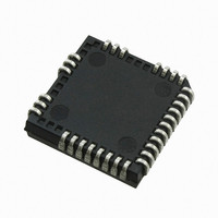
IRS26302DJPBF International Rectifier, IRS26302DJPBF Datasheet - Page 30

IRS26302DJPBF
Manufacturer Part Number
IRS26302DJPBF
Description
IC BRIDGE +1 GATE DVR 3PH 44PLCC
Manufacturer
International Rectifier
Datasheet
1.IRS26302DJTRPBF.pdf
(51 pages)
Specifications of IRS26302DJPBF
Configuration
3 Phase Bridge
Input Type
Non-Inverting
Delay Time
320ns
Current - Peak
200mA
Number Of Configurations
1
Number Of Outputs
3
High Side Voltage - Max (bootstrap)
600V
Voltage - Supply
10 V ~ 20 V
Operating Temperature
-40°C ~ 125°C
Mounting Type
Surface Mount
Package / Case
44-PLCC (32 Leads)
Number Of Drivers
6
Driver Configuration
Non-Inverting
Driver Type
High and Low Side
Input Logic Level
CMOS/TTL
Rise Time
190ns
Fall Time
75ns
Propagation Delay Time
710ns
Peak Output Current
350mA
Power Dissipation
4.6W
Operating Supply Voltage (min)
10V
Turn Off Delay Time
50ns
Turn On Delay Time (max)
50ns
Operating Temp Range
-40C to 125C
Operating Temperature Classification
Automotive
Mounting
Surface Mount
Pin Count
32
Package Type
PLCC
Lead Free Status / RoHS Status
Lead free / RoHS Compliant
Available stocks
Company
Part Number
Manufacturer
Quantity
Price
Company:
Part Number:
IRS26302DJPBF
Manufacturer:
International Rectifier
Quantity:
10 000
Separate Logic and Power Grounds
The IRS26302DJ has separate logic and power ground pin (V
noise problems that can occur in power conversion applications. Current sensing shunts are commonly used in many
applications for power inverter protection (i.e., over-current protection), and in the case of motor drive applications, for
motor current measurements. In these situations, it is often beneficial to separate the logic and power grounds.
Figure 26 shows a HVIC with separate V
V
ITRIP pin and the V
output voltage used to drive the low-side gate is V
output voltage of the driver minus the drop across R
Tolerant to Negative V
A common problem in today’s high-power switching converters is the transient response of the switch node’s voltage
as the power switches transition on and off quickly while carrying a large current. A typical 3-phase inverter circuit is
shown in Figure 27; here we define the power switches and diodes of the inverter.
If the high-side switch (e.g., the IGBT Q1 in Figures 28 and 29) switches off, while the U phase current is flowing to
an inductive load, a current commutation occurs from high-side switch (Q1) to the diode (D2) in parallel with the low-
side switch of the same inverter leg. At the same instance, the voltage node V
voltage to the negative DC bus voltage.
www.irf.com
SS
is used as the reference point for the logic and over-current circuitry; V
SS
pin. Alternatively, the COM pin is the reference point for the low-side gate drive circuitry. The
S
Transients
Figure 26: Separate V
SS
and COM pins and how these two grounds are used in the system. The
LO
G,LO
-COM; the gate-emitter voltage (V
.
30
SS
and COM pins
SS
R
R
2
and COM respectively) to eliminate some of the
1
R
0
X
in the figure is the voltage between the
S1
, swings from the positive DC bus
GE
) of the low-side switch is the
© 2009 International Rectifier
IRS26302DJ


