IRS26302DJPBF International Rectifier, IRS26302DJPBF Datasheet - Page 3
IRS26302DJPBF
Manufacturer Part Number
IRS26302DJPBF
Description
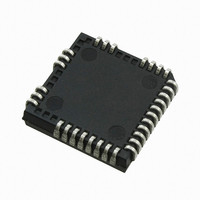
IC BRIDGE +1 GATE DVR 3PH 44PLCC
Manufacturer
International Rectifier
Datasheet
1.IRS26302DJTRPBF.pdf
(51 pages)
Specifications of IRS26302DJPBF
Configuration
3 Phase Bridge
Input Type
Non-Inverting
Delay Time
320ns
Current - Peak
200mA
Number Of Configurations
1
Number Of Outputs
3
High Side Voltage - Max (bootstrap)
600V
Voltage - Supply
10 V ~ 20 V
Operating Temperature
-40°C ~ 125°C
Mounting Type
Surface Mount
Package / Case
44-PLCC (32 Leads)
Number Of Drivers
6
Driver Configuration
Non-Inverting
Driver Type
High and Low Side
Input Logic Level
CMOS/TTL
Rise Time
190ns
Fall Time
75ns
Propagation Delay Time
710ns
Peak Output Current
350mA
Power Dissipation
4.6W
Operating Supply Voltage (min)
10V
Turn Off Delay Time
50ns
Turn On Delay Time (max)
50ns
Operating Temp Range
-40C to 125C
Operating Temperature Classification
Automotive
Mounting
Surface Mount
Pin Count
32
Package Type
PLCC
Lead Free Status / RoHS Status
Lead free / RoHS Compliant
Available stocks
Company
Part Number
Manufacturer
Quantity
Price
Company:

Part Number:
IRS26302DJPBF
Manufacturer:
International Rectifier
Quantity:
10 000


IRS26302DJ
Description
The IRS26302DJPBF are high voltage, high speed power MOSFET and IGBT drivers with three independent high
and low side referenced output channels for 3-phase applications. An additional low side driver is included for PFC
or Brake IGBT driving operation. Proprietary HVIC technology enables rugged monolithic construction. Logic inputs
are compatible with CMOS or LSTTL outputs, down to 3.3V logic. Three current trip functions that terminate all
seven outputs can be derived from three external shunt resistors. Each overcurrent trip functions consists of
detecting excess current across a shunt resistor on DC+ bus, on DC- bus and on Brake or PFC circuitry. An enable
function is available to terminate all outputs simultaneously and is provided through a bidirectional pin combined
with an open-drain FAULT pin. Fault signal is provided to indicate that an overcurrent or undervoltage shutdown
has occurred. Overcurrent fault conditions are cleared automatically after an externally programmed delay via an
RC network connected to the RCIN input. A diagnostic feature can give back to the controller the fault cause
(UVcc, DC- or DC- overcurrent) and address a fault register. The output drivers feature a high pulse current buffer
stage. Propagation delays are matched to simplify use in high frequency applications designed for minimum driver
cross conduction. The floating channel can be used to drive N-channel power MOSFET’s or IGBT’s in the high
side configuration which operates up to 600 V.
Simplified Block Diagram
www.irf.com
© 2009 International Rectifier
3
Related parts for IRS26302DJPBF
Image
Part Number
Description
Manufacturer
Datasheet
Request
R

Part Number:
Description:
SCHOTTKY RECTIFIER
Manufacturer:
International Rectifier Corp.
Datasheet:
Part Number:
Description:
SCHOTTKY RECTIFIER
Manufacturer:
International Rectifier Corp.
Datasheet:
Part Number:
Description:
SCHOTTKY RECTIFIER
Manufacturer:
International Rectifier Corp.
Datasheet:
Part Number:
Description:
SCHOTTKY RECTIFIER
Manufacturer:
International Rectifier Corp.
Datasheet:
Part Number:
Description:
SCHOTTKY RECTIFIER
Manufacturer:
International Rectifier Corp.
Datasheet:
Part Number:
Description:
SCHOTTKY RECTIFIER
Manufacturer:
International Rectifier Corp.
Datasheet:
Part Number:
Description:
SCHOTTKY RECTIFIER
Manufacturer:
International Rectifier Corp.
Datasheet:
Part Number:
Description:
SCHOTTKY RECTIFIER
Manufacturer:
International Rectifier Corp.
Datasheet:
Part Number:
Description:
SCHOTTKY RECTIFIER
Manufacturer:
International Rectifier Corp.
Datasheet:
Part Number:
Description:
SCHOTTKY RECTIFIER
Manufacturer:
International Rectifier Corp.
Datasheet:
Part Number:
Description:
SCHOTTKY RECTIFIER
Manufacturer:
International Rectifier Corp.
Datasheet:
Part Number:
Description:
SCHOTTKY RECTIFIER
Manufacturer:
International Rectifier Corp.
Datasheet:
Part Number:
Description:
SCHOTTKY RECTIFIER
Manufacturer:
International Rectifier Corp.
Datasheet:
Part Number:
Description:
SCHOTTKY RECTIFIER
Manufacturer:
International Rectifier Corp.
Datasheet:
Part Number:
Description:
SCHOTTKY RECTIFIER
Manufacturer:
International Rectifier Corp.
Datasheet: